
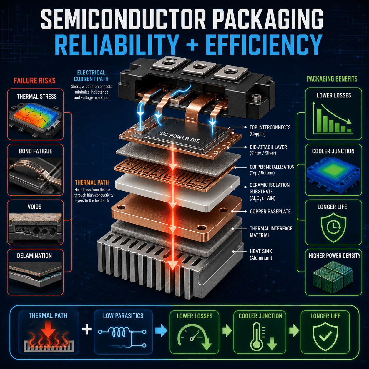
When evaluating a power semiconductor module, it is easy to focus on the device technology inside, silicon IGBTs, silicon carbide MOSFETs, or fast-recovery diodes. Yet the semiconductor die is only one part of the performance equation.
The package surrounding it determines how current reaches the die, how quickly heat escapes, how much unwanted inductance enters the switching loop, and how well the assembly survives temperature changes, vibration, moisture, and electrical stress.
In many power-electronics applications, packaging is what determines whether an advanced semiconductor reaches its full potential, or becomes the weakest link in the converter.
Semiconductor Packaging Is More Than an Enclosure
A power module package performs several jobs simultaneously. It must:
- Provide reliable electrical connections
- Carry high current with minimal resistance
- Insulate high voltage from the cooling surface
- Transfer heat away from the semiconductor junctions
- Protect internal components from contamination and moisture
- Absorb mechanical and thermal stress
- Maintain safe clearance and creepage distances
- Support precise, repeatable installation
These requirements frequently compete with one another. Thicker insulation may improve voltage isolation but increase thermal resistance. Rigid joints may transfer heat efficiently but experience greater mechanical stress during temperature changes.
Effective packaging balances these factors for the module’s intended voltage, current, environment, and operating life.
Inside a Typical Power Module
A conventional power module may contain:
- Semiconductor dies
- A die-attach layer
- Top-side electrical interconnections
- Copper circuit patterns
- An electrically insulating ceramic substrate
- A baseplate or direct cooling interface
- Power and signal terminals
- Encapsulation material
- A protective housing
Every layer and connection affects performance. A module can fail even when its semiconductor junctions remain within their published electrical ratings if an internal joint, wire bond, substrate, or insulation system deteriorates.
How Packaging Influences Conduction Loss
The semiconductor is not the only source of resistance. Current must also pass through internal traces, joints, bond wires, clips, lead frames, and external terminals.
The power dissipated by those resistances is:
Conduction loss = current² × resistance
Because current is squared, small reductions in package resistance can produce meaningful efficiency improvements at high load.
For example, an interconnection resistance of just 0.5 milliohm produces 125 watts of loss at 500 amperes.
Modern packages reduce resistance through:
- Thicker copper conductors
- Shorter current paths
- Wide lead frames
- Copper clips
- Parallel interconnections
- Double-sided current paths
- Optimized terminal layouts
Lower interconnection resistance also reduces internal heating, which can improve both semiconductor performance and package life.
How Packaging Influences Switching Loss
Every internal conductor has parasitic inductance. When current changes rapidly, this inductance generates voltage according to:
Induced voltage = inductance × rate of current change
During switching, parasitic inductance can cause:
- Voltage overshoot
- Current overshoot
- Oscillation and ringing
- Increased switching loss
- Electromagnetic interference
- False gate-driver signals
- Uneven current sharing
- Additional stress on insulation and semiconductor junctions
To control these effects, engineers may be forced to slow the switching transition. That reduces overshoot but increases the time during which the device simultaneously carries current and supports voltage, raising switching loss.
A low-inductance package allows cleaner and potentially faster switching. Common design features include:
- Short internal connections
- Closely coupled positive and negative conductors
- Wide, flat current paths
- Laminated structures
- Symmetrical die placement
- Kelvin gate-drive connections
- Integrated DC-link connections
Package inductance is especially important for silicon carbide and gallium nitride devices, whose fast switching can expose weaknesses that were less significant with slower silicon devices.
The Value of Kelvin Connections
In a conventional module, the gate driver and main load current may share part of the same source or emitter path. Rapid changes in load current create a voltage across that shared inductance, altering the effective voltage seen by the gate.
This can slow switching, create oscillation, or contribute to unintended turn-on.
A Kelvin-source or Kelvin-emitter terminal gives the gate driver a separate reference connection that does not carry the main load current. This provides more accurate control over the device and can improve:
- Switching consistency
- Noise immunity
- Current sharing
- Short-circuit protection
- Gate-voltage measurement
- Overall converter efficiency
The external gate-driver layout must preserve this advantage. Connecting the Kelvin terminal incorrectly can reintroduce the shared inductance the package was designed to avoid.
Packaging Defines the Thermal Path
Nearly all semiconductor losses become heat. The package must move that heat from the junction to the heat sink or coolant.
A typical thermal path is:
Junction → die attach → copper layer → ceramic substrate → lower copper layer → baseplate → thermal interface → cooling system
Each layer contributes thermal resistance. Each interface can also contain voids, delamination, contamination, or uneven contact.
Lower thermal resistance can provide:
- Lower junction temperature
- Higher usable output current
- Greater overload capability
- Reduced cooling requirements
- Improved power density
- Longer component life
The thermal path must also distribute heat evenly. A low average temperature does not guarantee reliability if one die or one area of a die develops a severe hot spot.
Steady-State and Transient Thermal Performance
Datasheets often provide junction-to-case thermal resistance, but steady-state resistance is only part of the thermal picture.
Short power pulses depend on transient thermal impedance. During a brief event, heat initially remains close to the active region of the die. As the pulse continues, it spreads through the substrate and package.
A module may tolerate a short overload that would be impossible continuously. Repetitive pulses, however, can accumulate heat before the package returns to its original temperature.
Reliable design should consider:
- Pulse duration
- Duty cycle
- Starting temperature
- Switching and conduction losses
- Cooling-system response
- Temperature variation among dies
- Transient thermal impedance
Average power alone may conceal damaging junction-temperature peaks.
The Role of the Insulated Substrate
The substrate carries current, supports the semiconductor dies, transfers heat, and provides electrical isolation.
Two common technologies are direct-bonded copper and active-metal-brazed substrates.
Direct-bonded copper
Direct-bonded copper, or DBC, consists of a ceramic layer bonded between copper layers. The copper forms the electrical circuit while the ceramic provides insulation and transfers heat.
Common ceramic materials include:
- Aluminum oxide
- Aluminum nitride
- Silicon nitride
Aluminum oxide is economical but has comparatively modest thermal conductivity. Aluminum nitride offers better heat transfer. Silicon nitride provides strong mechanical performance and is well suited to applications involving severe thermal cycling.
Active-metal brazing
Active-metal-brazed, or AMB, substrates use a brazing process to join copper to ceramic. This technology is frequently paired with mechanically strong ceramic materials for demanding high-power applications.
Substrate selection affects thermal resistance, insulation, fatigue life, manufacturability, and cost. No single material is best for every module.
Why Die Attach Matters
The die-attach layer joins the semiconductor to the substrate. It must carry heat and, in many designs, electrical current while withstanding repeated expansion and contraction.
Traditional modules often use solder. Over many temperature cycles, solder can develop:
- Fatigue cracks
- Voids
- Delamination
- Increased thermal resistance
- Localized hot spots
Silver-sintered attachment has become an important alternative in high-performance modules. A properly manufactured sintered joint can provide strong thermal conductivity, high-temperature capability, and improved power-cycling life.
Other approaches include diffusion bonding, transient liquid-phase bonding, and advanced solder systems.
The technology alone does not guarantee a reliable joint. Surface preparation, pressure, temperature, void control, material compatibility, and manufacturing consistency remain critical.
Wire Bonds and Their Failure Modes
Many conventional modules use multiple aluminum wires to connect the top surface of the semiconductor die to the package conductors.
Wire bonding is proven and economical, but the bond wires experience repeated electrical and mechanical stress.
As the die heats and cools, differences in thermal expansion can produce:
- Bond-wire lift-off
- Cracking at the bond foot
- Heel cracking
- Increased electrical resistance
- Unequal current distribution
- Local overheating
These effects can become self-reinforcing. A damaged bond carries less current, forcing the remaining bonds to carry more. Their temperature rises, accelerating further damage.
Improved wire-bond designs may use optimized patterns, thicker wires, copper wires, ribbons, or more fatigue-resistant attachment methods.
Copper Clips and Planar Interconnections
A copper clip replaces numerous small bond wires with a broad conductor attached across the top of the die.
Potential advantages include:
- Lower electrical resistance
- Lower package inductance
- Better current distribution
- Improved heat spreading
- Greater current capacity
- Fewer individual interconnection points
Planar interconnections take this idea further by using flat conductive structures, flexible circuits, or deposited layers.
These designs can improve efficiency and reliability, but they require careful management of attachment quality, mechanical stress, insulation, and manufacturing tolerances.
Single-Sided and Double-Sided Cooling
Traditional modules usually remove heat through the bottom of the semiconductor assembly. Double-sided cooling creates an additional thermal path from the top of the die.
Double-sided designs can:
- Reduce junction temperature
- Improve temperature uniformity
- Increase current capacity
- Reduce module size
- Increase power density
- Lower cooling-system requirements
This construction is increasingly useful in compact, high-power applications such as traction inverters.
Its benefits come with added design complexity. Cooling surfaces, insulation, die attachment, flatness, and mechanical pressure must all be controlled carefully.
Baseplate and Baseplate-Free Construction
A metal baseplate provides mechanical support and helps spread heat before it reaches the heat sink or cold plate.
However, it also adds another layer and often another bonded interface. These can increase thermal resistance, weight, and susceptibility to fatigue.
Baseplate-free modules place the insulated substrate more directly against the cooling surface. This can shorten the thermal path and reduce weight, but it makes the installation more sensitive to:
- Cold-plate flatness
- Surface finish
- Mounting pressure
- Thermal-interface thickness
- Clamping sequence
- Mechanical distortion
The best construction depends on the module, cooling system, assembly process, and expected operating environment.
Thermal Expansion Drives Mechanical Fatigue
Module materials expand at different rates when their temperature changes.
Silicon, silicon carbide, copper, aluminum, ceramic, solder, encapsulant, and baseplate materials each have different coefficients of thermal expansion. Because these materials are bonded together, their movement is constrained.
Repeated expansion and contraction can produce:
- Die-attach fatigue
- Substrate cracking
- Delamination
- Wire-bond damage
- Baseplate deformation
- Terminal fatigue
- Encapsulation separation
Designers reduce these stresses through material selection, compliant layers, optimized geometry, improved attachments, and temperature control.
Both maximum temperature and temperature swing matter. A module that repeatedly cycles through a large temperature range may wear faster than one that remains at a relatively stable temperature.
Power Cycling and Thermal Cycling
These two stresses are related but not identical.
Power cycling
Power cycling occurs when semiconductor losses repeatedly heat and cool the dies as load changes. It primarily stresses local structures such as wire bonds, top-side connections, and die attach.
Thermal cycling
Thermal cycling occurs when the temperature of the entire module changes because of ambient conditions, coolant variation, startup, or shutdown. It places greater stress on larger package interfaces, substrates, baseplates, terminals, and seals.
A module may perform well in one type of test but poorly in the other. Qualification and life estimates should reflect the application’s actual operating profile.
Environmental Protection
Encapsulation protects the semiconductor assembly from moisture, contamination, corrosive gases, and mechanical damage.
Common materials include:
- Silicone gels
- Molded compounds
- Resins
- Conformal coatings
- Sealing systems
The encapsulant must provide electrical insulation while remaining compatible with temperature cycling and the internal materials.
Moisture or ionic contamination can contribute to:
- Corrosion
- Leakage current
- Electrochemical migration
- Insulation deterioration
- Partial discharge
- Gate-circuit instability
A module housing should not be assumed to provide complete environmental isolation. Moisture can gradually diffuse through many polymers, making enclosure climate control and condensation prevention important.
High Voltage and Partial Discharge
High-voltage modules must maintain adequate insulation both through materials and across surfaces.
Important considerations include:
- Clearance
- Creepage distance
- Ceramic thickness
- Encapsulant quality
- Internal voids
- Contamination level
- Altitude
- Electric-field concentration
- Switching transients
Small voids within insulation can experience partial discharge. Each event may be too small to cause immediate breakdown, yet repeated activity can gradually erode the insulation.
Fast voltage transitions also drive capacitive and common-mode currents through the package. A module intended for high-speed silicon carbide operation must therefore manage transient electric fields as well as nominal voltage.
Current Sharing Inside the Module
High-current modules often contain several semiconductor dies operating in parallel. The package must give those dies similar electrical and thermal conditions.
Current sharing can be disturbed by differences in:
- Internal path resistance
- Gate-loop inductance
- Die temperature
- Threshold voltage
- Switching speed
- Thermal resistance
- Device characteristics
If one die carries more current, it may heat faster and experience greater electrical stress. Depending on the device and operating condition, that can further increase the imbalance.
Symmetrical internal layouts, balanced gate paths, Kelvin connections, effective heat spreading, and controlled manufacturing tolerances help the dies share current more predictably.
Packaging and Silicon Carbide Performance
Silicon carbide MOSFETs can switch faster and operate at higher temperatures than conventional silicon IGBTs. Those capabilities place more demanding requirements on the package.
The package must manage:
- High heat flux from relatively small dies
- Fast current transitions
- High rates of voltage change
- Low gate-voltage margins
- Short fault-withstand times
- Greater insulation stress
- Strong electromagnetic coupling
If package inductance is too high, the device may need to be switched slowly to control overshoot and ringing. That sacrifices part of the efficiency benefit that justified using silicon carbide.
Low-inductance current paths, Kelvin terminals, sintered attachments, advanced substrates, and improved cooling help the package keep pace with the semiconductor technology.
Packaging’s Effect on System-Level Efficiency
An advanced package can improve more than the module’s measured electrical loss.
Better thermal and electrical performance may enable:
- Higher switching frequency
- Smaller inductors and transformers
- Reduced snubber requirements
- Smaller heat sinks
- Lower fan or pump power
- Higher inverter power density
- Reduced system weight
- Greater overload capacity
Package improvements can therefore influence the size, cost, and efficiency of the complete converter.
Packaging’s Effect on Reliability
Module reliability improves when the package reduces both average stress and repeated stress.
Important reliability-enhancing features may include:
- Low-resistance interconnections
- Low-inductance layouts
- Strong ceramic substrates
- Sintered die attach
- Clip or planar top-side connections
- Uniform heat spreading
- Double-sided cooling
- Reliable environmental sealing
- Controlled electric fields
- Integrated temperature sensing
The complete design still matters. A sophisticated module can fail prematurely if it is installed on an uneven cold plate, operated beyond its cycling capability, exposed to condensation, or connected through a high-inductance bus.
Warning Signs of Package Degradation
Package deterioration may appear as:
- Rising on-state voltage
- Increasing thermal resistance
- Higher junction or case temperature
- Changing switching waveforms
- Unequal current sharing
- Increased ringing
- Intermittent electrical behavior
- Declining insulation resistance
- Partial-discharge activity
- Terminal discoloration
- Cracking or delamination
Some damage is invisible from outside. Specialized evaluation methods include X-ray inspection, acoustic microscopy, thermal-structure analysis, partial-discharge testing, power cycling, and destructive cross-section analysis.
For operating equipment, trending electrical and thermal parameters can reveal gradual change before complete failure.
What to Compare When Selecting a Module
Voltage, current, and power ratings are only the beginning. Package-related evaluation should also consider:
- Junction-to-case thermal resistance
- Transient thermal impedance
- Internal stray inductance
- Kelvin-terminal availability
- Die-attach technology
- Top-side interconnection method
- Substrate material
- Baseplate construction
- Insulation rating
- Partial-discharge performance
- Creepage and clearance
- Power-cycling capability
- Temperature-cycling capability
- Humidity and vibration qualification
- Mounting requirements
- Recommended thermal-interface material
Published performance should be reviewed under the stated test conditions. Ratings based on an ideal case or coolant temperature may not be achievable in the real enclosure.
Installation Is Part of the Package System
Packaging performance depends on correct integration.
Critical installation factors include:
- Proper mounting torque
- Correct tightening sequence
- Flat cooling surfaces
- Controlled thermal-interface thickness
- Low-inductance busbar layout
- Close placement of DC-link capacitors
- Short gate-drive connections
- Mechanically supported terminals
- Uniform coolant distribution
- Condensation prevention
Uneven mounting can create poor thermal contact or mechanically stress the ceramic substrate. Rigid external conductors can transfer vibration and thermal expansion into module terminals.
The module, busbar, gate driver, cooling system, and mechanical assembly should be treated as one engineered structure.
Match the Package to the Mission Profile
A module used in an uninterruptible power supply experiences different stresses from one used in an electric vehicle or wind turbine.
Selection should reflect the real mission profile, including:
- Load-current distribution
- Switching frequency
- DC-link voltage
- Overload duration
- Ambient and coolant temperatures
- Junction-temperature swings
- Startup and shutdown frequency
- Humidity and contamination
- Altitude
- Vibration
- Expected service life
- Fault frequency and severity
The most suitable package is not necessarily the one with the highest current rating. It is the one that can survive the application’s combined electrical, thermal, mechanical, and environmental stresses.
Common Misconceptions
“The semiconductor die determines efficiency.”
The die is central, but package resistance, inductance, cooling, and current sharing can significantly change total module loss.
“Low thermal resistance guarantees long life.”
Low thermal resistance helps, but fatigue, temperature cycling, insulation quality, mechanical stress, and environmental exposure also determine reliability.
“Silicon carbide automatically makes a converter more efficient.”
Silicon carbide offers substantial advantages, but inadequate packaging and layout may force slower switching or create excessive electrical stress.
“A sealed-looking module is immune to moisture.”
Moisture may still diffuse through polymeric materials or enter through imperfect interfaces.
“If average temperature is acceptable, the module is safe.”
Localized hot spots and large temperature swings can cause damage even when average temperature looks reasonable.
The Bottom Line
Semiconductor packaging technology directly influences module reliability, efficiency, and usable power.
It controls electrical resistance, switching inductance, heat transfer, current sharing, insulation strength, and resistance to environmental and mechanical stress. Advanced substrates, sintered die attach, copper clips, Kelvin connections, planar interconnects, and double-sided cooling can all improve performance when applied correctly.
The package must also be integrated with an appropriate bus structure, gate driver, cooling system, and mechanical assembly. A strong semiconductor in a poorly designed package, or a well-designed module installed incorrectly, will not deliver dependable performance.
When comparing modules, look beyond the semiconductor material and headline ratings. The package is the physical system that allows the die to carry current, switch efficiently, reject heat, and survive years of operation. In many applications, it is the package, not the die, that ultimately sets the limits.