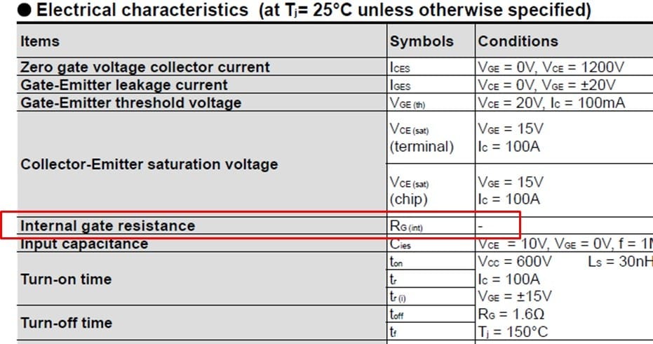
“Refer to the data sheet where internal gate resistance (RG) values for the 6th-generation V-series and 7th-generation X-series IGBT module are described.
Please contact us with a model type number if it is not shown in the 6th-generation data sheet or if it is a product prior to the 6th-generation (U-series, S-series).”
FAQ Categories: Driver Design
-
What ohm value is set for internal gate resistance (RG) in an IGBT module?
-
How can the surge voltage be reduced?
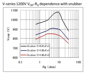
A surge voltage is generated by high di/dt, and wiring inductance outside the module, at the time of switching (L*di/dt). Some of the ways to suppress this problem are as follows:
(1) Add a protective circuit
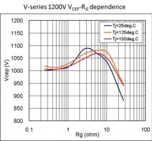
(2) Reduce di/dt by adjusting RG or –VGE
(3) Reduce inductance by making the main circuit wiring thicker and shorter, and using a copper bar and parallel flat wiring
For details, refer to Application Manual Chapter 5.


-
How should the gate resistance (RG) be determined?
The gate resistance value (RG) greatly impacts dv/dt, radiation noise, voltage/current surge, and switching loss. Please comprehensively determine an appropriate value that corresponds to the target figure of your actual design. As for reference, a recommended turn-on resistance value (RG(on)) is twice or higher than that of the standard value from datasheet, and a recommended turn-off resistance value (RG(off)) is one to two times that of the standard value.
-
Is it always expedient to use the gate resistance (RG) value indicated in the data sheet?
The optimum gate resistance value (RG) varies depending on the circuit configuration or operating environment used. The data sheet describes the recommended resistance value to minimize switching loss. Determine an appropriate gate resistance (RG) after considering the relevant switching loss, EMC/EMI, surge voltage, and unexpected characteristics such as vibration, without deviating from the descriptions contained in the data sheet.