Comments Off on Are there any measures to prevent misfiring by high dv/dt during the reverse recovery of the FWD?
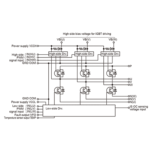
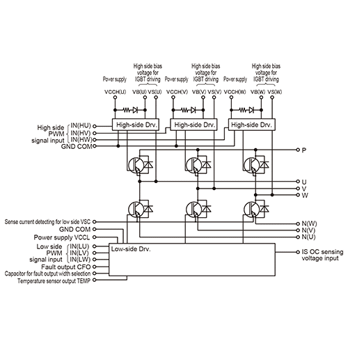
Some of the ways to prevent misfiring of an IGBT are as follows: (1) by adding a capacity component CGE to the area between the gate and emitter (2) by increasing –VGE (3) by increasing gate resistance (RG) The effectiveness of these measures will vary depending on the applicable gate circuit, so please verify thoroughly […]
Comments Off on What precautions do I need to be aware of when connecting IGBT modules in parallel?
There are four basic precautions, shown below, when connecting IGBT modules in parallel: (1) Current unbalance control during steady operation (2) Current unbalance control at the time of switching (3) Gate drive circuit (4) Derating For details, refer to Application Manual Chapter 4-3.5 and Chapter 8.
One way to determine the validity of the dead-time setting is to verify the current on the direct current power line during non-loading time. For details, refer to Application Manual Chapter 7.
Comments Off on How can we determine the dead-time?
To prevent a short-circuit in the upper and lower arms, it is necessary to set an on-off timing delay between the several arms. During this time period both devices are switched off. The dead-time needs to be set so that it is generally longer than the switching time of the IGBT (toff max.). For details, […]
Comments Off on Which parameters have an impact to IGBT’s short-circuit current?
IGBT’s short-circuit current is impacted by gate-to-emitter voltage VGE, junction temperature Tj, and switching voltage Vcc. Generally, a short-circuit current increases with a large VGE, low Tj, and large Vcc.
Comments Off on What precautions need to be considered when designing an IGBT drive circuit?
Refer to Application Manual Chapter 7-5. It provides precautions regarding the photo-coupler’s noise capability, wiring between the drive circuit and IGBT, and gate overvoltage protection.
Comments Off on Can application of a reverse-bias voltage (-VGE) on a gate-to-emitter be exempted in a case where only an FWD is used without an opposite IGBT, such as in a chopper circuit?
Please apply a reverse-bias voltage (-VGE) of -5 V or higher (-15 V recommended; max. -20 V) between the gate and emitter in the IGBT that is not being used. An insufficient reverse-bias voltage (-VGE) may cause the IGBT to misfire due to dV/dt at the time of reverse-recovery of the FWD, resulting in damage. […]
Comments Off on What is the reason for applying reverse-bias voltage (-VGE) between the gate and emitter?
An insufficient reverse-bias voltage (-VGE) between the gate and emitter may cause the IGBT to mis-fire, leading to a short-circuit current. If the current is cut off the surge voltage and the generated loss may damage the product. For details, refer to Application Manual Chapters 4-3.3 and 7-1.2.
Comments Off on What are the points we need to be aware of when determining the gate resistance (RG)?
A larger gate resistance (RG) will increase switching loss, and make it more prone to generating an arm short circuit due to an insufficient dead-time. A smaller gate resistance (RG)may cause a sudden surge voltage. For details, refer to Application Manual Chapters 2-2.2 and 7-1.3.
Restaurant Industry Solutions
An installation of 3 of our FRENIC-Ace inverters and an HMI with connection via MODBUS was implemented in a restaurant in Croatia to offer customers a 360º view of the city. The task was to control the motors that are simultaneously rotating the restaurant platform, avoid any failures, and analyze and collect feedback of the application.
Our inverters control 3 of their motors, offering power control, protection against failures, speed control and maintenance warnings. Meanwhile, our HMI gives access to analytic data like current, temperature, and more at any moment.
Cleaning machines for kitchens, heaters, and air conditioners have an electric brushing solution which enters deep into ventilation ducts. Their rotating, flexible shafts must adapt perfectly to their environment without causing any damage. Fuji Electric installed our FRENIC-Mini C2 inverters into those cleaning machines, as well as our Monitouch Technoshot HMI screens.
The HMI replaced all manual keypads and push buttons and therefore modernized the machines significantly. With the FRENIC-Mini C2 and its quick response torque limitation, the cable inside the hose as well as the duct is well protected. In addition, the StopGo system stops the motor way before any breakdown can occur!
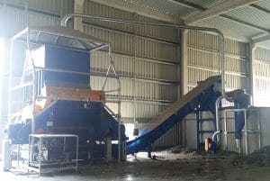
We installed our FRENIC-MEGA inverters in a garbage recycling shredder that has 2 motors of 132 kW, mechanically coupled in the same axis. The main requirements in this application were a high starting torque (overload up to 200%), a control in the load imbalance and the maintenance of speed during the process.
With our FRENIC-MEGA and its “droop-control” function, we can keep the load unbalance to a minimum. This represents a machine process control without stops, thus prolonging its maintenance!
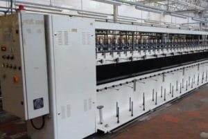
We installed our FRENIC-Ace, 3-phase 400 V, 1.5 to 2.2 kW into a textile machine in Italy. The challenge was to control a permanent magnetic synchronous motor (PMSM) in open loop and to find a function to stop the machine with PID function in case of input phase loss.
Our solution provides a low voltage ride-through function, a best PMSM control with static pole-tuning at starting, and which has CANopen built-in.
For this installation, Fuji Electric developed a complete cabinet with EPLAN schematics. 2 FRENIC-Ace inverters with our special software for solar pumping (CLI-SOL) were installed: 1 inverter of 7.5 kW for submersible pumps (irrigation pump) and 1 inverter of 2.2 kW for water rotation pump of the lake.
A third standard FRENIC-Ace inverter was also installed for synthetic main supply, which allows the connection of any other external 230/400V AC load.
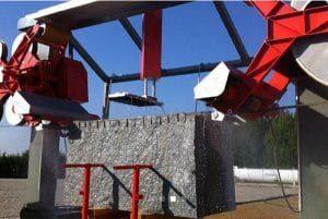
Our HMI Monitouch Technoshot allow a remote connection through VNC, so you can watch, read and save the information of the inverter and PLC of your installation or machine. This is an installation of diamond wire saw machine for cutting and processing natural stone in quarries, such as granite, marble, slate, onyx, etc.
As well as for industrial materials such as metals, composites, glass, PVC. Now our customer could upgrade and go from a totally manual process (with buttons) to a more automated and visual process!
When doing maintenance on an Uninterruptible Power Supply and its auxiliary equipment, keeping it clean is one of the main objectives. Dirt, dust, sawdust, and metal filings are just some of the pollutants that technicians see in UPSs, even when installed in seemingly clean environments. These substances can cause failures when they contaminate the contacts of relays and contactors, and conductive material can cause short circuits and malfunctions on printed circuit boards (PCBs).
At least once a year, make sure your UPS gets cleaned including a good vacuuming with a non-conductive hose and attachments. Never use a blower or compressed air! These methods can blow contaminants deeper into the unit, causing real troubleshooting headaches if and when they finally do cause issues.
Use lint-free rags lightly damp with a nonflammable and fast-drying solvent for heavy deposits, and soft brushes around delicate components and connectors. Always perform cleaning work on equipment that is offline, and de-energized and with the proper personal protective equipment (PPE) such as goggles, gloves, aprons, and respirators as necessary. Lastly, always use a torque wrench on copper and lead connectors
Close
Optimize Your HMI.
Fit more on a screen! Did you know that you can show and hide screen parts like Switches and Displays according to memory addresses and security levels? When in detail settings, click on Other Settings in the bottom left and be sure that Show/Hide is checked. Then go to that panel and change as you’d like
The power of one touch! Did you know you can assign Macros to switches? Run hundreds of lines of code on the rising and falling edge of any switch in your application, all with one finger press!
Your data in your hands! Did you know that V-Server can pull data to a SQL database from PLCs through a Monitouch HMI going back decades. PLC-5? SLC-502? Easy as uploading the application and selecting the PLC memory addresses and your SQL database locations.
With Monitouch’s expansive catalogue of drivers and strong SCADA abilities, old machines can be modernized for data collection while keeping the controls cabinet. This cuts cost and holds uptime.
Close
Know Your Pipe and Don't Guess
Know your pipe and don't guess! This includes the customer knowing their liner and its thickness. Many customers don't know their pipe's exact specifications, but by measuring circumference and looking for a schedule embossment on a fitting, as well as referencing a pipe resource is usually a good solution.
It is also something they can research with a system engineer ahead of a flow survey or fixed installation. To that point, they could even program the measurement point(s) on the bench in air conditioning before going in the field.
Close
Optimize Your Inverters
Clean your drive fans and filters often - this keeps them cool and running longer!
You can find detailed information on the communication registers (S codes, M codes, etc.) in the RS485 User's Manual. This information also applies to Ethernet based communications.
Frenic-ACE needs destination set up at first powering up, make sure you select USA(5) by press "Func/Data" key at 8.dES display. Then while press and hold "STOP" key, use arrow key to change it from Asia(2) to USA (5)
Check the application notes on our website!
Close
Get Your Installation Right
Surveying the intended installation location for straight run, and selecting a valid installation point is one of the most important tips we could offer. That is after vetting Transit Time Ultrasonic technology for the macroscopic application. This is by far the biggest battle we have in the field, even when we try to get this information upfront in our application work.
It seems that people use the basic rule of 10D up/5D down and apply it to all situations, or make no straight run considerations at all. I would highlight the need for additional straight runs for the plumbing situations that poses the biggest obstacles for us. The biggest being pumps, two elbows out of plane, valves, and T fittings. The trick is to portray this without evoking fear, just to bring them to conscious thought.
Close
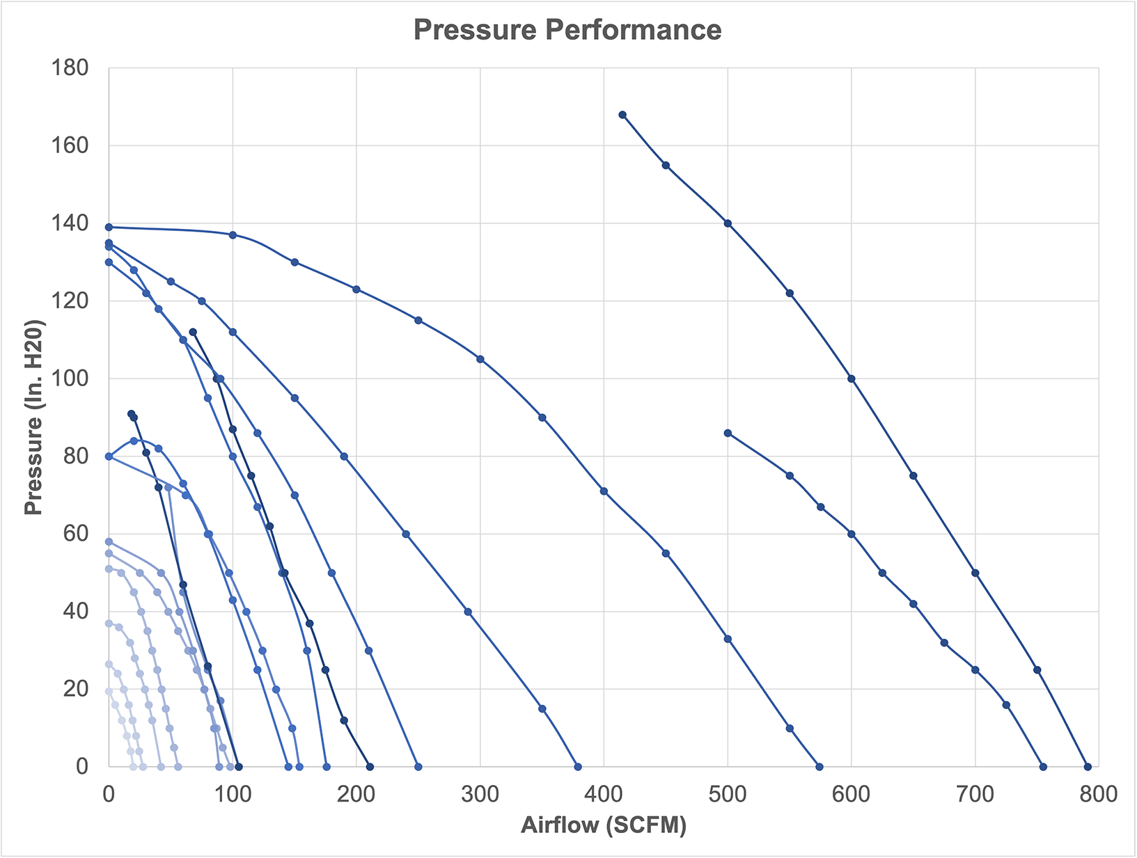
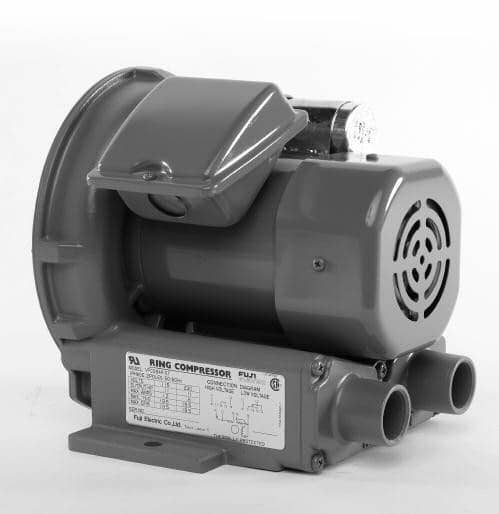
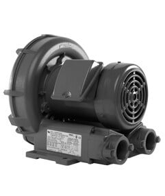
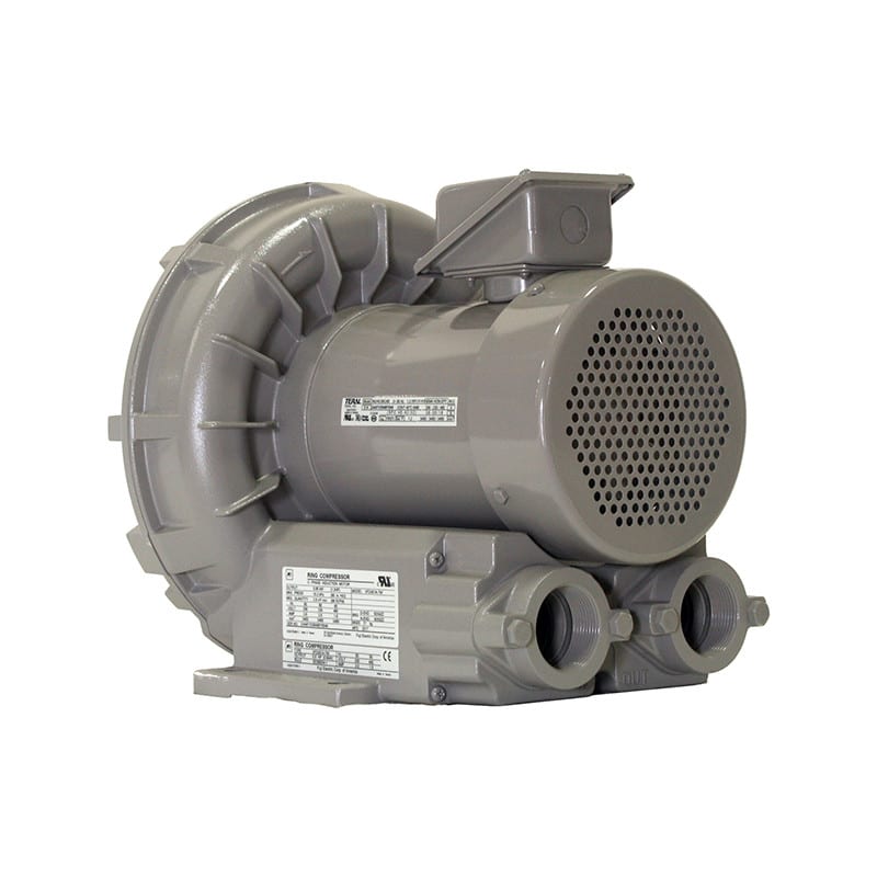
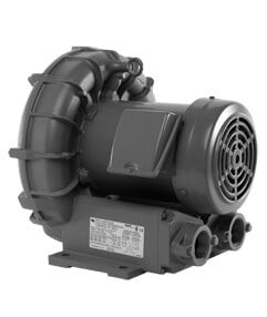
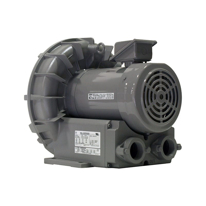
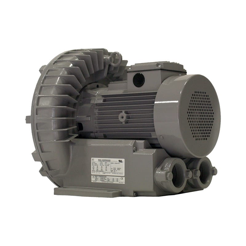
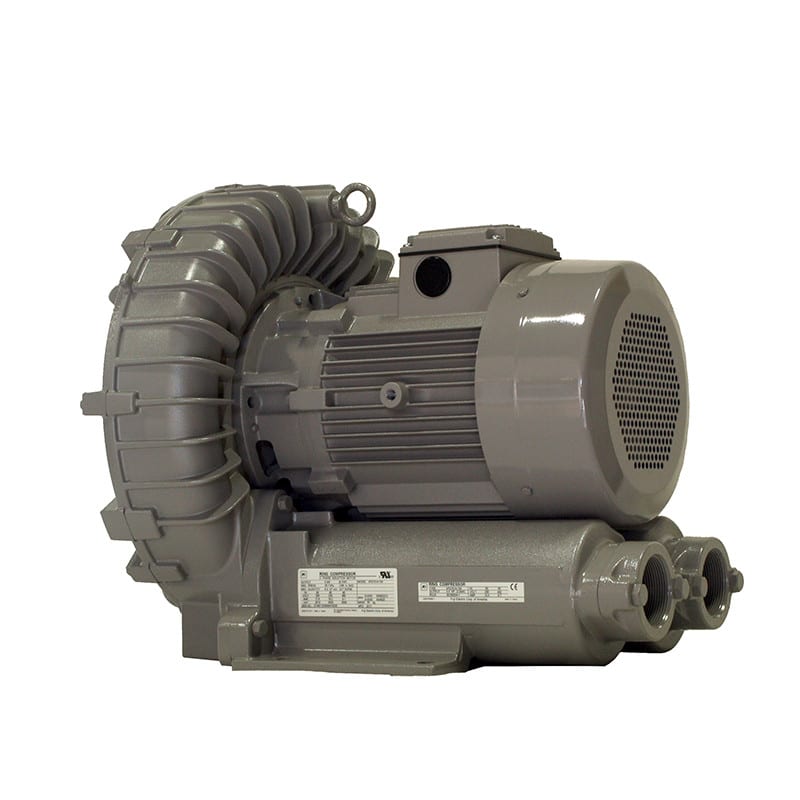
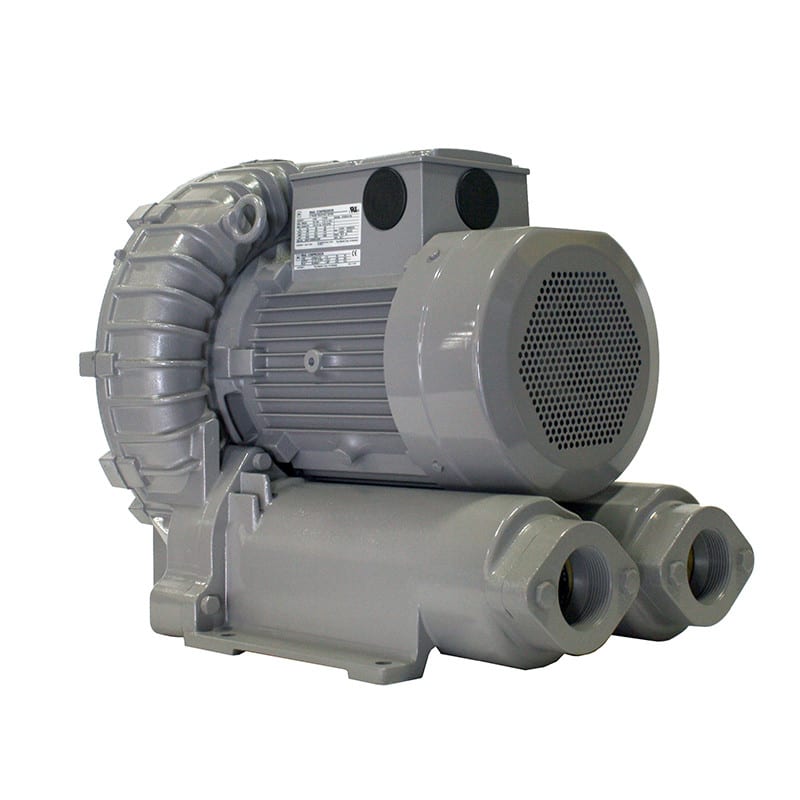
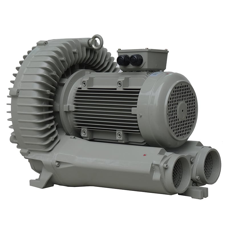
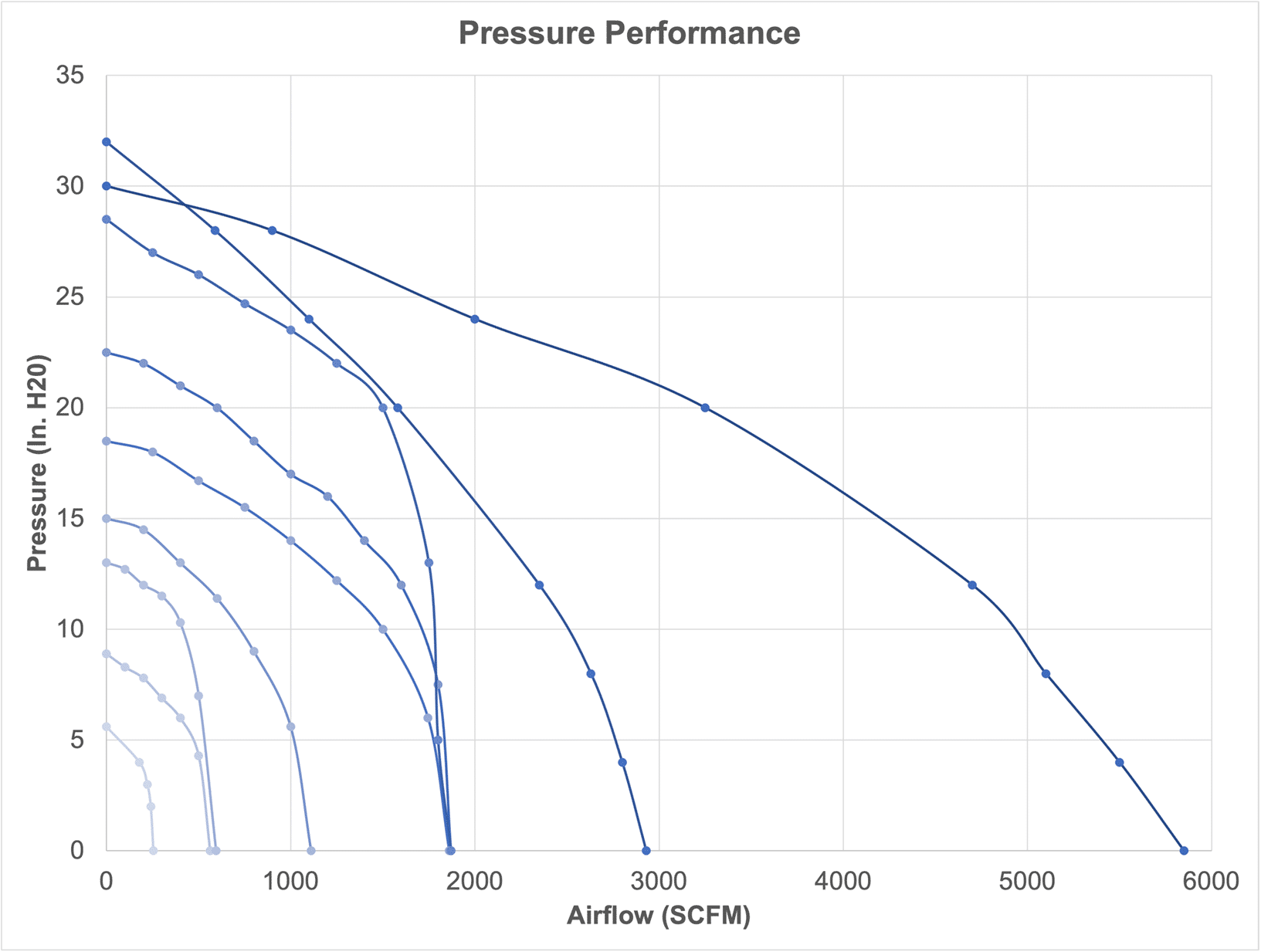
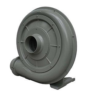
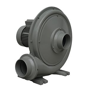
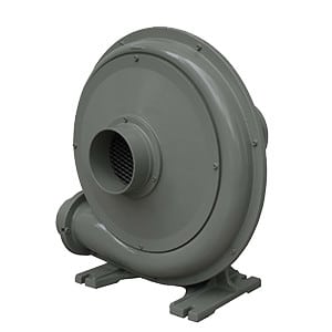
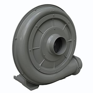
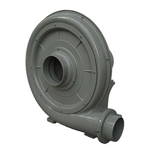
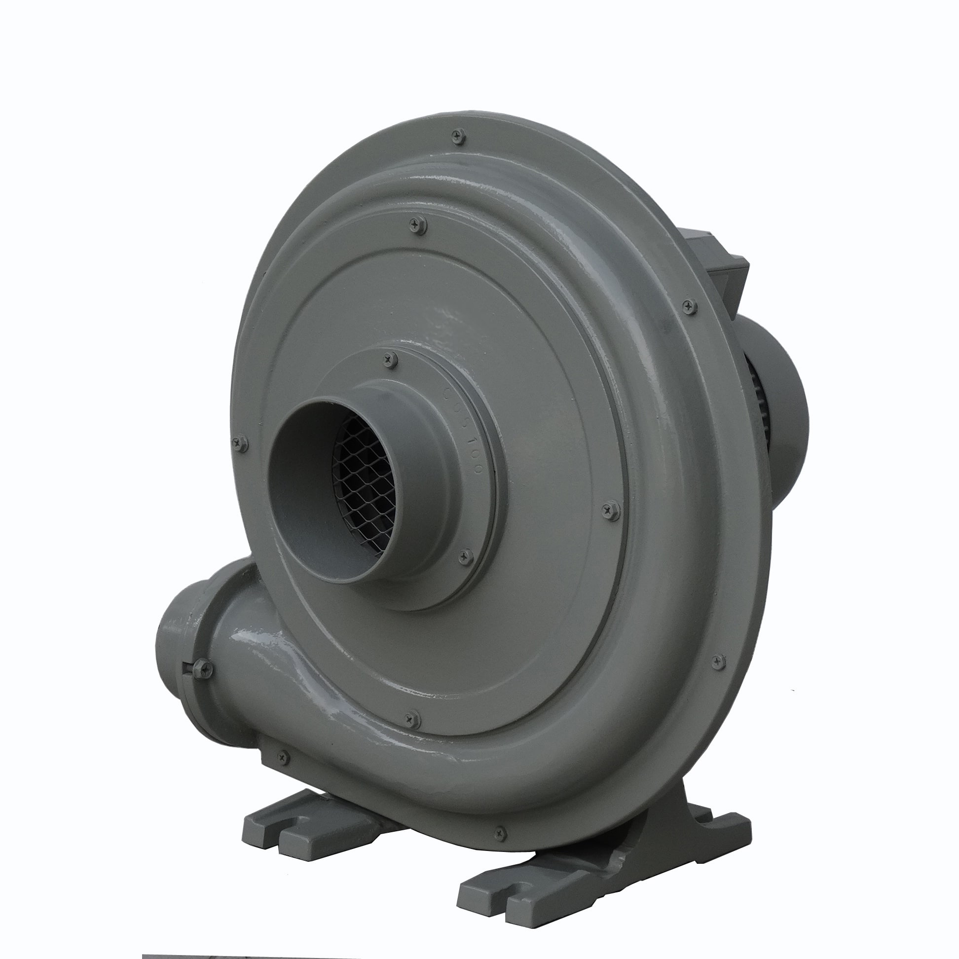
Ring Compressors & Blowers for Pressure, Vacuum, and Airflow
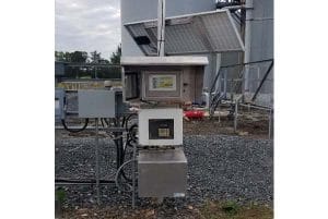
Pressure Systems for Waste Water Treatment and Aquaculture rely on Fuji Electric Regenerative Blowers to provide reliable pressure. For Waste Water applications, our blowers provide airflow and pressure for aeration of Waste Water Systems. In Aquaculture, our blowers provide airflow for pressure application in the aeration tanks for Shrimp and Fish.
Vacuum Applications for Pneumatic Tube Systems and Hold Down Applications for Milling & Cutting utilize Fuji Electric Regenerative Blowers for its vacuum capabilities. Fuji Electric Blowers provide reliable pressure and vacuum as the driver for Tube systems. Our regenerative blowers also provide vacuum for hold down applications for milling and cutting applications.
Airflow & Aeration When it comes to efficient and reliable airflow, industries such as Metal Plating and Commercial Spas & Hot Tubs use our blowers. Fuji Electric Regenerative blowers provide aeration for plating tanks, mixing tanks and rinsing tanks. Our blowers also provide aeration for commercial spas and hot tubs.
We understand you need products to be reliable and manufactured to the highest quality standards. In this case, when a large volume manufacturer of residential elevators was experiencing widespread field failures with their current supplier of the VFD used in their application, they immediately sought out an alternative solution.
Our engineering team and resources at the customer worked in concert to provide a comprehensive solution that required meeting the highest quality standards in their industry. A solution was provided and tested over 800,000 cycles. Several competitor’s products failed during the testing process. Fuji Electric was selected as their primary source for their production requirements and adopted as their standard of choice. At Fuji Electric, we pride ourselves on manufacturing products that exceed our customers expectations.
Compact size and shallow mounting depth make Fuji Electric operator interfaces ideal for installation in harsh environments, and for many factory automation applications. Did you know Fuji Electric HMI’s are utilized in the Oil and Gas – Test and Measurement industry? We work with companies who selected several manufacturers to test; several of those failed to pass their stringent harsh duty requirements.
After months of field operation, Fuji Electric was chosen as their preferred choice to meet their application requirements. Since then, we have deployed several thousand units in the field, operating in the most extreme temperature climates. When choosing Fuji Electric for your HMI requirements, you can be assured of receiving a product that is suitable for just about any industrial environment!
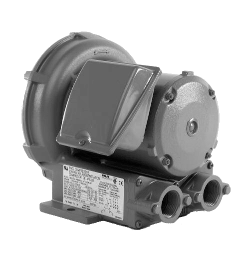
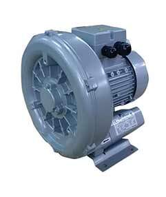
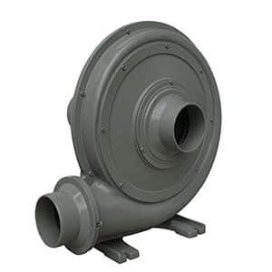
Most spas and hot tubs require regenerative blowers to provide the pressure and flow needed to agitate the water. Here are your Do’s & Don’ts for your Commercial Spa to operate smoothly:
Do’s 1. Use a licensed electrician to install your blower. 2. Use a Pressure relief valve. 3. Use a Hartford loop at least 18 inches above the water level of the spa. 4. Install the blower as close to the spa as possible. 5. Install the blower in a weatherproof house or enclosure. 6. Install a check valve as close to the spa as possible. 7. Install an Inlet Filter on the blower.
Don’ts 1. Don’t install the unit lower than the water level of the spa. 2. Don’t allow water into the blower. Water will damage the blower and void the warranty
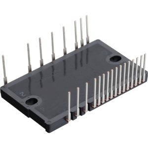
Semiconductors that Keep Your Production Line Moving
Welding is a critical activity used on many modern production lines. So, when downtime hits, your entire line can go down. Our IGBT modules have been specifically designed to maximize uptime so you don't miss a step.
Low Loss Reduce inverter loss by 10% and chip temperature by 1 OC compared with the 6th generation V series EP3 Package (75A at fc = 8kHz).
Miniaturization An approximately 36% smaller footprint has been achieved by reducing power loss and improving heat transfer
High Temperature Operation Up to 35% more output than the previous generation. A 2x improvement in power cycle capability.
Your UPS prevents system shutdown during power outages by relying on IGBT modules. Our IGBT modules offer the right characteristics to keep everything up and running.
High Reliability Achieves continuous operation at 175°C through chip optimization and heat resistance of package to minimize field failures.
High Efficiency Thinning the thickness and miniaturizing the structure of the IGBT chip and diode chip reduces power losses during inverter operation.
The nation’s largest manufacturer of turn-key, automated car wash systems chose Fuji Electric as their standard of choice for all of their AC Drives requirements. Our product offering supplies them the efficiency and reliability required for every aspect of automating their processes.
The customer tested several manufacturers over a decade ago and found that Fuji Electric surpassed their expectations in keeping their systems running that impacted their profitability due to low maintenance requirements and longer uptime. Our cost effective, compact solutions met their design requirements to include the 3-year warranty that differentiated Fuji Electric from other manufacturers.
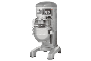
A long standing customer that tested several competitors’ products over a decade ago, chose a Fuji Electric product that not only meets their application criteria, but exceeded their expectations regarding: performance, quality and reliability for their commercial mixer product lines.
As their standard of choice, our AC Drives continue to surpass expectations as our product models offer the versatility and flexibility required for any demanding environment. Fuji Electric AC Drives prove to be technically superior compared to other products offered in the market. Our compact design, 3-year warranty, and exceptional torque features is ideal for many recipe requirements that make Fuji Electric their sole supplier for all of their AC drives needs.
Our products are designed to operate in 50 deg C ambient under full load conditions with no derating factor. The VFDs also maintains a UL rating under single phase power input. Fuji Electric’s ECO-DY model has a standard feature of a simultaneous control of Pump pressure and water table level control. This feature will control a pump’s output pressure and automatically switch to water table level control when the level sensor goes below an adjustable threshold. This prevents costly dry run damage to the submersible pump.
Fuji Electric VFDs are designed to handle harsh outdoor conditions needed for Agriculture Irrigation control. For this case, the ECO-DY model achieves the control by switching between two PID loops. Throughout this process, the first loop, PID1, will control the output pipe pressure. The second loop, PID2, controls the water table level. There is a sensor threshold and time that controls the switching between PID1 or PID2. One of the PID sensors will need to be a 0-10v signal and the second will need to be a 4-20ma input.
Fuji Electric VFDs are a tough, rugged and designed to operate in the harsh conditions of the oil field. Our VFDs are used in thousands of Oil field pump jack applications. For this Oil Field application, they run in 50 deg C ambient at full power without derating.
In this application, our VFDs provided the standard capability to overcome the regeneration portion of the pump jack cycle without needing braking resistors. Our VFD accurately senses the regenerative energy created by the beam pump and precisely increases the speed to eliminate the need for a braking resistor.
Peter Pugger is the world’s leading manufacturer of mixing extruders (pugmills). With the growing demand to mix and extrude new and innovative products, Peter Pugger machines require versatility and efficiency as it relates to motor control, speed control, soft start/stop and remote capability. The utilization of Fuji Electric's FRENIC-Mini and FRENIC-ACE drives has allowed their systems to maintain product quality, durability and performance. The durability of our Fuji Electric drives and the three-year warranty has established our drives as the drive of choice for all of our units. With thousands of machines worldwide, Fuji Electric’s dependability has played a key role in their success.
H2O Technologies is a high quality, highly innovative OEM Control Panels fabricator that specializes in the engineering, designing and building of Bypass Control Panels for hydraulic pump related industries that construct fountains, waterfalls and municipal pools. Fuji Electric’s FRENIC -Eco and EcoPAK Bypass Panels quickly became H2OTechnologies’ exclusive offering due to its high quality, product adaptability, and superb technical & support staff. “We have discovered a hidden gem working with Fuji Electric; it’s their ability to take us back to better days, when there was less bureaucracy, where management decisions and issues resolution were local and only a phone call away. That is a “game-changer” that sets them far apart from almost every other large organization”, exclaims Greg Sills, PPX Central’s President & CEO.
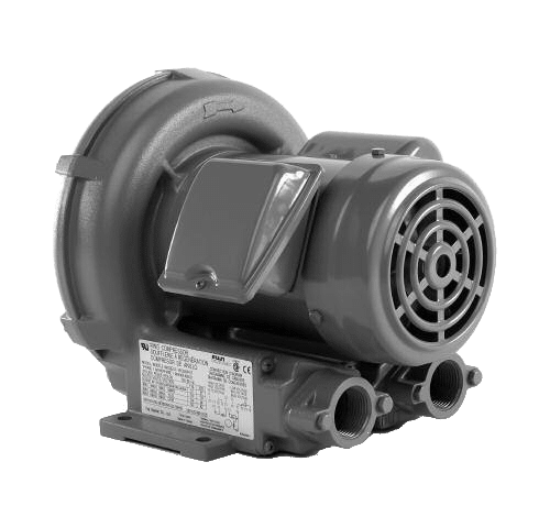
Fuji Regenerative Blowers are used to provide Air agitation for Plating, Cleaning and Rinse Tanks. They can provide high amounts of air at low pressures. They offer the advantages of clean, oil-free air that does not deliver any contaminants to foul or spoil the tank fluid. Fuji Regenerative Blowers offer a form of agitation without any moving parts in the bath. Blowers require no lubrication and that means no contaminated chemical baths. Fuji Blowers are dependable and reliable devices with no wearing, rubbing or sliding components.
Fuji Electric Power Semiconductors are used in Wind Turbines of major Wind Turbine Manufacturers. The PrimePACK™ 3+ improves power conversion efficiency to reduce power loss and increase output power. Amid the beautiful and expansive natural landscape of northern Denmark, you can see lines of wind turbines. These wind turbines use our large-capacity IGBT module PrimePACK™ 3+. In this wind power generation, the force of wind spins the blades of the wind turbine, which in turn rotates the generator to generate electricity. In order to feed this electricity into transmission lines, the voltage and frequency must be changed, and that power conversion is where our power semiconductors play a vital role.
Fuji Electric VFDs are designed to handle harsh outdoor conditions needed to run Electric Submersible pumps (ESPs) in the Oil Field. They operate in 50 deg C ambient under full load conditions with no derating factor. VFDs also maintain a UL rating under single phase power input.
For ESPs, Fuji Electric’s FRENIC-Mega is packaged in a Nema 3R enclosure along with a sine wave filter that feeds a step up transformer to create the high voltage needed for the special ESP motor. The ESP motor is sometimes thousands of feet down in the well bore. Some ESP motors are induction style while others are permanent magnet style. The Fuji Electric FRENIC-Mega works on both types of ESPs. Fuji Electric's VFD has a special feature that allows motor base voltage at speed to be adjusted while monitoring current for maximum operating efficiency thus saving valuable electrical power operation costs.
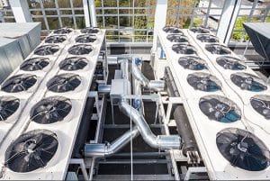
Significant levels of refrigerants and heating are needed to slow down spoilage and maintain preharvest freshness and flavor of ripe fruit and vegetables. Fuji Electric Variable Frequency Drives (VFD) make it possible to quickly provide the necessary cooling or heating to maintain a uniform temperature, humidity, air-circulation or fresh air requirements in cold storage while at the same time the energy consumption is reduced to a minimum. In standard system designs, electric motors are intended to operate at a fixed speed. This speed is determined by the frequency of the power supply and the motor design (number of poles).
The shaft load on the motor is determined by the product of shaft speed and torque. With a fixed speed, motor power is determined by the torque of the load. With a change in speed the motor load will not only benefit from the speed reduction, but also any reduction in torque with speed. Two types of motor load exist; constant torque and variable torque.
VFDs give better control and more efficiency for compressors, fans and pumps:
VFD speed control will reduce the power penalty associated with slide valve, poppet valve or throttling capacity control. On compressors with no capacity control speed control will eliminate other poor control strategies.
VFD speed control provides dramatic fan power reductions at reduced speed. This also translates into reduced motor heat loads in refrigerated spaces.
VFD speed control provides dramatic fan power saving relative to fan cycling
For maintenance of AC Drives, it is best to institute a schedule of routine maintenance which includes cleaning of the drives and their heatsinks. This prevents overheating and also prevents other debris from being lodged inside the drive!
Close
Scheduling a Freight Pick Up
A customer was given incorrect information for scheduling a freight pick up and the terms for shipping the item. The shipment was delayed and stuck in a freight branch location. This led our team to coordinate communications between several stakeholders (Customer, Logistics Company, End User, and the freight company shipping the order). Information had to be confirmed for accuracy and ease of understanding to avoid confusion or delays. Our team at Fuji Electric was able to keep the customer informed of status regularly and get the info needed in order to resolve the issue and get the order completed.
Close
Meeting Production Schedules
Due to material challenges, in order to meet our customer's production schedule, our team members participate in weekly meetings, provide status and shipping updates, and facilitate direct shipments from our factories. It requires daily attention and time management skills to keep track of multiple avenues to achieve delivery. However, there is a great sense of satisfaction knowing we are part of a team doing everything possible to meet their expectations!
Close
Critical Need of Our Parts
An auto supplier was in critical need of parts or they go line down. Our team called members from Fuji Electric Japan's shipping team and got them to move an ocean orders to air drop ship to customer. No lost downtime!
Did you also know Fuji Electric Corp. of America (FECOA) was established in 1970? Fuji Electric Corp. of America is happy to celebrate over 50 years in the United States! Fuji Electric now aims to become a leading-edge company in “energy and the environment” by building upon our core platform of five technology fields which unlock the potential of electricity—energy, industrial systems, social systems, power electronics, and electronic devices.
Close
Industrial Laundry Solutions
Fuji Electric’s FRENIC-Ace model, Variable Frequency Drives (VFDs) are commonly used in commercial laundry equipment for their ability to control the speed of electric motors. In the context of commercial laundry, VFDs are often employed in various machines and systems to enhance efficiency, reduce energy consumption, and provide better control over operations. Here are some ways VFDs are utilized in commercial laundry equipment.
Motor Control: Can regulate the speed of electric motors in washers, dryers, extractors, and other laundry equipment. By adjusting the motor speed according to the load and operational requirements, VFDs help optimize energy consumption and extend the lifespan of the equipment.
Energy Efficiency: Enable soft starts and stops, reducing the energy demand during motor acceleration. They also allow for precise control of motor speed, preventing unnecessary energy consumption when full speed is not required. This contributes to energy savings and overall operational efficiency.
Customized Washing Cycles: In laundry equipment, different fabrics and loads may require varying levels of agitation, spin speed, or drying time. VFDs provide the flexibility to customize washing cycles by adjusting motor speeds, ensuring that each load is treated appropriately.
Load Balancing: Used to balance loads in commercial laundry systems. VFDs contains an algorithm that detects and corrects an imbalance of wet material in the washing drum to prevent damaging vibrations during the spin-drying cycle.
Maintenance Benefits: By controlling motor speed and providing real-time performance data, VFDs can contribute to predictive maintenance strategies. Monitoring motor parameters allows for early detection of issues, reducing downtime and preventing costly equipment failures.
Environmental Compliance: The ability of VFDs to control motor speed based on demand aligns with energy efficiency requirements and environmental regulations. Using VFDs in commercial laundry equipment helps businesses meet sustainability goals and adhere to energy efficiency standards.
In summary, Variable Frequency Drives play a crucial role in enhancing the performance, energy efficiency, and operational flexibility of commercial laundry equipment. They contribute to cost savings, reduce environmental impact, and improve the overall reliability of laundry systems.