Mainly the turn-off loss Eoff will be affected. As –VGE increases, Eoff decreases.
FAQ Categories: Driver Design
-
Why does Fuji recommend to connect a resistor between G-E terminals of IGBT terminal?
If voltage is applied between C-E while the gate is open, the divided voltage by Cres and Cies is applied to the gate, as well. This may lead to a gate breakdown from overvoltage, or a breakdown by heating from elevated device temperature due to a unstable ON state of the gate. As such, for the inverter circuit, the sequence where voltage between C-E is applied after gate circuit is established is recommended. Even if this sequence is not set up, a resistor inserted between G-E to stabilize the gate potential will help to avoid this breakdown phenomenon. In that case, a resistance of about 10kΩ against open (infinite resistance) is recommended. If the resistance is too small, you will see problems such as lower gate voltage than the designed value and an increased current consumption in the drive circuit (because the gate voltage will be the one divided with gate resistance RG.) Therefore, a resistance sufficiently low against the open value is enough and you don’t need to change it according to the current rating of the device.
-
We like to configure a bootstrap circuit for the upper arm control power supply of a small IPM outside the module as well. Is there any problem?
This is not problematic. Small IPM modules already contain bootstrap diodes and a limiting resistor inside.
-
What is the recommended dead time for an IGBT module and an IPM, respectively?
Fuji recommends a dead time larger than 3 μs for IGBT module. For IPMs dead time should be larger than 1 μs.
-
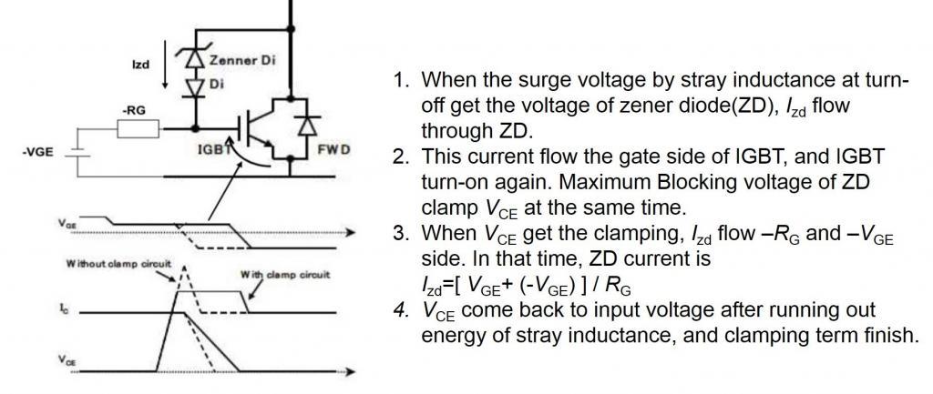
What is the active clamp circuit?
It is a protection circuit, added to suppress a surge voltage between the collector and the emitter.

-
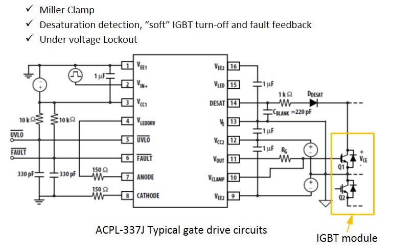
Is there any way to simplify the design of the gate drive circuit for the IGBT module and furthermore, include the protection circuit?
IGBT gate drive ICs are supplied from many companies including BROADCOM, Renesas Electronics, Texas Instruments, ISAHAYA ELECTRONICS and TOSHIBA. As the ICs contain short-circuit protection and voltage drop protection circuits within the chip, design of the drive circuit will be simplified. An IGBT module evaluation board with mounted drive IC is available. Please download the information and use it for your reference. However, Fuji Electric does not guarantee its characteristics when combined with an IGBT module.

-
What is the variance of the internal gate resistance (rg) in an IGBT module?
It is ±10%. However, it is not guaranteed.
-
What is the recommended value of the reverse-bias voltage (-VGE) between gate and emitter?
A range between -5V and -15V is recommended. With lower –VGE, the turn-off time toff becomes large and the turn-off loss Eoff increases. Additionally, the IGBT may misfire and cause a short-circuit current flow.
-
What is the dead time?
“To prevent a short-circuit in the upper and lower arms, it is necessary to set an on-off timing delay between the different arms. During the so called ‘dead time’ period both devices are switched off.
For details, refer to Chapter 7.3 of IGBT Module Application Manual.” -
Please let me know the carrier frequency characteristic of the control power supply consumption current of small PIM.
Please refer to the Technical Document of "Carrier frequency dependency of control power supply consumption current".