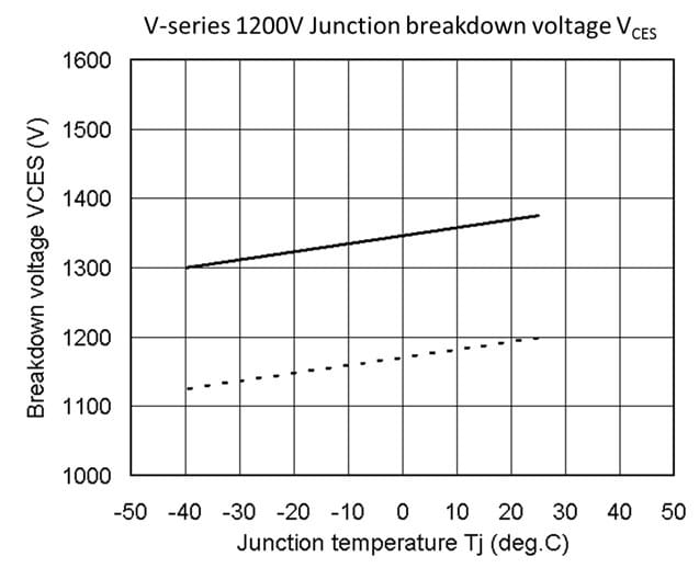
A lower temperature reduces the IGBT’s maximum collector-emitter voltage (VCES). The data sheet describes the maximum collector-emitter voltage (VCES) under the condition of Tj=25oC. Refer to the technical information describing temperature dependency included in the technical documents under Design Support.
FAQ Categories: IGBT Module
-
Is there a temperature dependency in the IGBT’s maximum collector-emitter voltage (VCES)?
-
Can an IPM operate at -40oC?
Our IPM is designed with a lowest guaranteed operating temperature of Tc=-20oC. Operation below this temperature has not been evaluated, and any use below -20oC will void your warranty. At such temperature, there are concerns about possible malfunctions due to a lower device withstand voltage or reduced capacity of the used capacitor.
-
What is the lowest operation temperature for an IGBT module?
The minimum temperature is specified by the storage temperature (Tstg). Please consider that there will be a reduced device withstand voltage and peripheral component (capacitor, control circuit) characteristics under low temperature before use.
-
What precautions need to be considered when designing an IGBT drive circuit?
Refer to Application Manual Chapter 7-5. It provides precautions regarding the photo-coupler’s noise capability, wiring between the drive circuit and IGBT, and gate overvoltage protection.
-
Can application of a reverse-bias voltage (-VGE) on a gate-to-emitter be exempted in a case where only an FWD is used without an opposite IGBT, such as in a chopper circuit?
Please apply a reverse-bias voltage (-VGE) of -5 V or higher (-15 V recommended; max. -20 V) between the gate and emitter in the IGBT that is not being used. An insufficient reverse-bias voltage (-VGE) may cause the IGBT to misfire due to dV/dt at the time of reverse-recovery of the FWD, resulting in damage.
For details, refer to Application Manual Chapter 3-10. -
What is the reason for applying reverse-bias voltage (-VGE) between the gate and emitter?
An insufficient reverse-bias voltage (-VGE) between the gate and emitter may cause the IGBT to mis-fire, leading to a short-circuit current. If the current is cut off the surge voltage and the generated loss may damage the product. For details, refer to Application Manual Chapters 4-3.3 and 7-1.2.
-
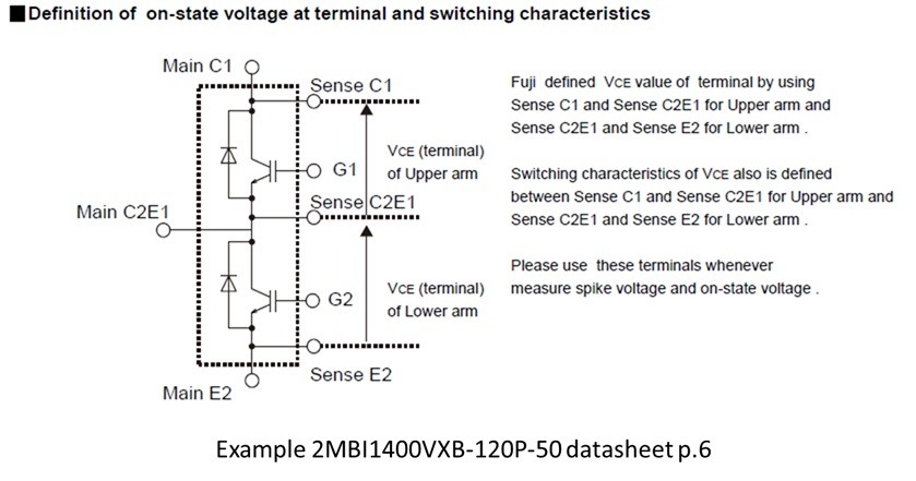
Which terminal should be used to measure the collector-emitter voltage (VCE) when switching?
Please measure at the main terminal of the product. If a terminal is separately specified for measurement in the data sheet, please use the specified terminal.

-
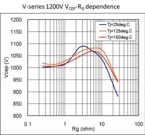
What are the points we need to be aware of when determining the gate resistance (RG)?
A larger gate resistance (RG) will increase switching loss, and make it more prone to generating an arm short circuit due to an insufficient dead-time. A smaller gate resistance (RG)may cause a sudden surge voltage. For details, refer to Application Manual Chapters 2-2.2 and 7-1.3.
-
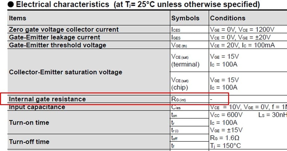
What ohm value is set for internal gate resistance (RG) in an IGBT module?
“Refer to the data sheet where internal gate resistance (RG) values for the 6th-generation V-series and 7th-generation X-series IGBT module are described.
Please contact us with a model type number if it is not shown in the 6th-generation data sheet or if it is a product prior to the 6th-generation (U-series, S-series).”

-
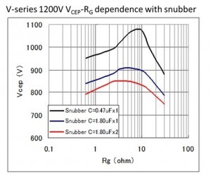
How can the surge voltage be reduced?
A surge voltage is generated by high di/dt, and wiring inductance outside the module, at the time of switching (L*di/dt). Some of the ways to suppress this problem are as follows:
(1) Add a protective circuit
(2) Reduce di/dt by adjusting RG or –VGE
(3) Reduce inductance by making the main circuit wiring thicker and shorter, and using a copper bar and parallel flat wiring
For details, refer to Application Manual Chapter 5.