
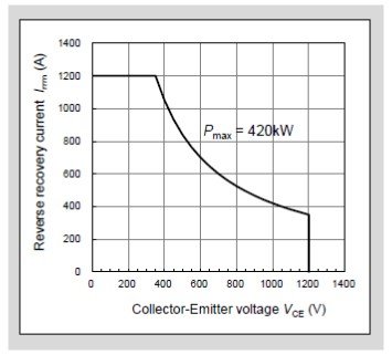
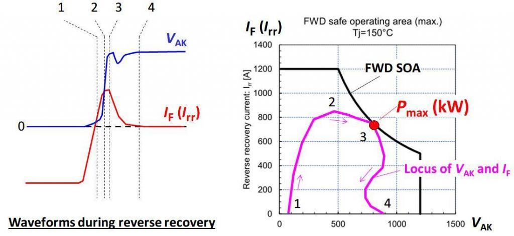
Similar to an IGBT, the FWD has a SOA (Safty Operating Area). Please refer to the following graph which is also shown in the product specifications. It displays an area that indicates the maximum allowed power Pmax. Since Pmax is the product of the voltage VAK applied during reverse recovery and the forward current IF, it limits these two parameters. The design should take into account the SOA and assures that the locus VAK–IF stays within the SOA. If power, exceeding Pmax, is applied, FWD may be damaged. In that case, take countermeasures like increasing the gate resistance of the IGBT ON-side, or using a snubber circuit to suppress the surge voltage.
Archives: FAQ
-
Does a Safety Operating Area for FWD (Free Wheeling Diode) exist?
-
The modules with press-fit pins, can they be pulled out and pressed in again?
It is not recommended.
-
What is the power cycle capability ΔTvj?
In operations where the junction temperature Tvj of a semiconductor chip changes, thermal stress is generated between the materials of the power module. Fatigue will be accumulated from repeated thermal stress, leading to breakdown in the end. Increasing temperature change ΔTvj, leads to a reduction in the lifetime of the power module. It is called as the power cycle capability ΔTvj.
-
What is the relation between switching loss and DC voltage VCC?
They are almost proportional. The switching loss increases as the DC voltage becomes higher.
-
What is the reason of power cycle capability ΔTj curve bending at 50oC?
ΔTj power cycle breakdown mode will become solder degradation mode in the operation with large temperature variation and wire peeling mode in the operation with relatively small temperature variation. Additionally, the transition from plastic to elastic behavior occurs at around 50oC, which causes an inflection point in the curve.
-
What is the recommended value of the reverse-bias voltage (-VGE) between gate and emitter?
A range between -5V and -15V is recommended. With lower –VGE, the turn-off time toff becomes large and the turn-off loss Eoff increases. Additionally, the IGBT may misfire and cause a short-circuit current flow.
-
What is the power cycle capability ΔTc?
Power cycle capability is the capability of the module to withstand repeated heating and cooling. The case temperature Tc will goes up and down until the modules fails: Stress strain is generated between the metal base plate and the insulating substrate causing fatigue in the solder under the insulating substrate. Refer to technical documents describing the relation of ΔTc and the expectancy of life of the device.
-
Is an evaluation board for the IGBT module available?
A board for characteristic evaluation of the module is available. Please contact Fuji Electric Corp. of America or your local sales representative or distributor to answer your question.