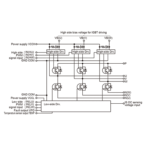
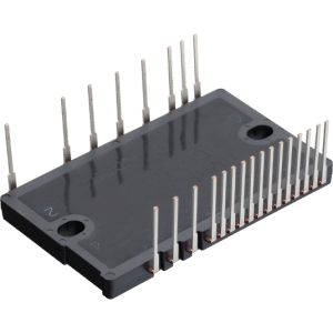
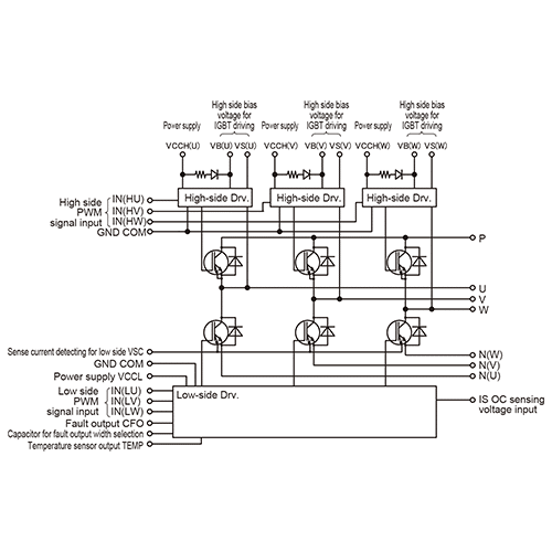
Designing an IGBT (Insulated Gate Bipolar Transistor) drive circuit involves careful consideration to ensure both the functionality and longevity of the device. Here are several key precautions that need to be considered: 
- Gate Drive Voltage: It’s crucial to ensure that the gate drive voltage is within the specified range for the IGBT. Exceeding the maximum gate voltage can damage the gate oxide layer, whereas insufficient gate voltage can prevent the IGBT from turning on fully, leading to higher conduction losses and potential overheating.
- Gate Resistance: Proper selection of gate resistance is essential. A lower gate resistance can speed up switching times but may lead to higher electromagnetic interference (EMI) and potential overshoots during switching, which can damage the IGBT. A higher gate resistance slows down the switching, reducing EMI but increasing switching losses.
- Protection against Overcurrent and Short Circuit: IGBTs are susceptible to damage under overcurrent conditions or short circuits. Incorporating protection mechanisms such as fuses, current sensors, or fast-acting shutdown circuits can help protect the IGBT from these extreme conditions.
- Temperature Monitoring: IGBTs can fail if operated beyond their maximum temperature limits. Including temperature sensors to monitor the heat sink or the IGBT itself and integrating thermal shutdown mechanisms are crucial to prevent thermal runaway.
- Snubber Circuits: To protect the IGBT from voltage spikes caused by parasitic inductances and to dampen oscillations, snubber circuits (RC or RCD snubbers) can be used across the collector-emitter terminals. These circuits absorb excess energy and smooth out the voltage waveform during switching events.
- Adequate Power Supply Decoupling: Good decoupling using capacitors close to the gate driver power supply pins is necessary to manage switching noise and provide a stable power supply, especially during fast switching transients.
- EMI Considerations: The high switching speeds of IGBTs can generate significant electromagnetic interference. Proper layout design, including minimizing loop areas, using twisted-pair wires for gate drives, and shielding sensitive components, can mitigate EMI effects.
- Dv/Dt and Di/Dt Control: Rapid changes in voltage (Dv/Dt) and current (Di/Dt) during switching can induce stress on the IGBT and surrounding components. Ensuring controlled switching through gate resistor tuning and careful circuit layout can help manage these rates to avoid component damage.
- Gate Driver Isolation: Isolation between the gate driver and the power circuit is essential to protect the control side from high voltages and currents. Optocouplers, transformers, or dedicated driver ICs with built-in isolation can be used for this purpose.
- Dead Time Management: In circuits where two IGBTs are connected in a half-bridge configuration, it’s essential to ensure that there is a sufficient dead time between turning off one IGBT and turning on the other to prevent a short circuit across the DC bus.
- PCB Layout: Careful consideration of the PCB layout is critical. Layout affects everything from signal integrity to thermal management. Ensure short, direct routing for critical connections, adequate spacing for high voltage traces, and effective thermal paths for heat dissipation.
By addressing these factors, you can enhance the reliability, efficiency, and safety of IGBT drive circuits, ensuring they function well within their operational limits and application requirements.


