The manufacturing of semiconductors is a highly complex and precise process involving multiple steps to convert raw materials like silicon into functional semiconductor devices, such as integrated circuits (ICs) or microchips. Below is an overview of the semiconductor manufacturing process: 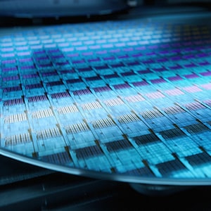
- Raw Material Preparation
- Silicon Extraction:
- Silicon, the primary material, is extracted from quartz or sand, which contains silicon dioxide (SiO₂).
- The silicon is purified to semiconductor-grade (99.9999% pure) through the Czochralski process or Float Zone process.
- Ingot Formation:
- Purified silicon is melted and formed into a cylindrical ingot or boule.
- The ingot is sliced into thin wafers using precision saws, and the surfaces are polished to a mirror finish.
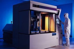
- Wafer Fabrication
This is the process of creating circuits on the silicon wafer. It involves several steps:
Oxidation
- A thin layer of silicon dioxide (SiO₂) is grown on the wafer surface to act as an insulator or protective layer.
- Oxidation is achieved by exposing the wafer to oxygen or water vapor at high temperatures.
Photolithography
- A photosensitive material (photoresist) is applied to the wafer.
- A mask or reticle with the desired circuit pattern is used, and ultraviolet (UV) light shines through the mask to expose the photoresist.
- The exposed regions of the photoresist are developed and washed away, leaving a pattern.
Etching
- The exposed areas of the wafer are etched using chemical or plasma processes to remove unwanted material.
- Etching can be:
- Wet Etching: Using liquid chemicals.
- Dry Etching: Using plasma or reactive gases.
Deposition
- Thin layers of material, such as metals or dielectrics, are deposited onto the wafer surface.
- Deposition methods include:
- Chemical Vapor Deposition (CVD).
- Physical Vapor Deposition (PVD).
- Atomic Layer Deposition (ALD).
Doping (Ion Implantation)
- Impurities (dopants) are introduced to the silicon wafer to modify its electrical properties, creating n-type or p-type regions.
- This is done by bombarding the wafer with ions of the dopant material in a controlled manner.
Planarization
- After multiple layers of patterning and deposition, wafers are planarized (flattened) using chemical-mechanical polishing (CMP) to ensure uniform thickness.
- Circuit Formation
- The wafer undergoes multiple cycles of photolithography, etching, and deposition to build layers of transistors, interconnects, and other components.
- Advanced chips may have dozens of layers to achieve high functionality.
- Testing and Inspection
- Electrical Testing:
- Probes test the circuits on the wafer to verify functionality and identify defects.
- Inspection:
- Optical and electron microscopy ensure the precision of patterns and layers.
- Defects are flagged for removal or correction.
- Wafer Dicing
- The wafer is sliced into individual semiconductor chips using precision saws or lasers.
- Packaging
- The individual chips are placed in protective packages to provide mechanical support and electrical connections.
- Packaging steps include:
- Die Bonding: Attaching the chip to a substrate.
- Wire Bonding or Flip-Chip Technology: Connecting the chip to external leads.
- Encapsulation: Sealing the chip in a plastic or ceramic package.
- Final Testing
- The packaged chips undergo rigorous testing to ensure they meet specifications for functionality, reliability, and performance.
- Distribution
- Chips are sorted and shipped to manufacturers for use in electronic devices, such as computers, smartphones, and automotive systems.
Advanced Techniques in Semiconductor Manufacturing
- Extreme Ultraviolet (EUV) Lithography:
- Used for creating smaller features on chips (e.g., 5nm or 3nm technology nodes).
- 3D Chip Stacking:
- Chips are stacked vertically to enhance performance and reduce size.
- High-K Dielectrics and Metal Gates:
- Materials used to improve transistor efficiency at smaller scales.
Challenges in Semiconductor Manufacturing
- Precision: Features are often smaller than 10 nanometers, requiring atomic-level accuracy.
- Yield: High defect rates can make manufacturing expensive.
- Equipment Costs: Fabrication facilities (fabs) require billions of dollars in investment.
In summary, semiconductor manufacturing is a multi-step process that transforms raw silicon into advanced electronic devices. Each step requires cutting-edge technology, precision engineering, and strict quality control to ensure the performance and reliability of the final product.