It stands for Insulated Gate Bipolar Transistor. It is a voltage-controlled device that has an insulated gate with an oxide insulating film. The gate structure is similar to a MOSFET. It combines the positive characteristics of a MOSFET and bipolar transistor. It is an indispensable component in a power conversion circuit for high-voltage and large-current applications. It is mainly used in consumer equipment such as air conditioners (a/c) or microwave ovens, industrial equipment such as elevators, and inverters for hybrid electric vehicles (HEV) and electric vehicles (EV).
2. Why is FWD required?
Conventional IGBT elements are not capable of blocking a reverse-withstand voltage. When an inverter circuit is used to drive an inductive load like in a motor, the load current will continue flowing in the reverse direction (emitter to collector) at the time of switching. This may damage the IGBT. The IGBT is protected by a commutating load current in a diode (freewheeling diode: FWD) connected inversely in parallel.
3. What is the difference between an IGBT and a MOSFET?
An IGBT is a device that has a basic structure of a P-layer added to the drain side of a MOSFET. An IGBT is suited for large-current and high withstand-voltage applications. A MOSFET is suited for small-capacity and high-speed switching applications.
4. What is a RB-IGBT?
It stands for Reverse Blocking Insulated Gate Bipolar Transistor. Reverse-parallel connection of RB-IGBT enables both way switching. It is incorporated in AT-NPC (Advanced T-type Neutral Point Clamped) 3-level inverters, to increase the power conversion efficiency because there are less current passing elements.
5. What does SiC mean?
It stands for Silicon Carbide. SiC has a wider bandgap width compared to silicon, and is expected to become the next-generation power device material for high-temperature operation, high-speed switching, low power-loss, and high withstand-voltage applications.
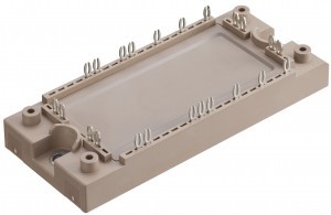
6. What is a module?
A module is a package which contains several power semiconductor devices that form a bridge circuit, etc. A modul provides thermal and electrical contact as well as the electrical insulation maintained between the heat-radiation surface and the electric part. For this reason multiple modules can be placed on the same heat sink. Compared to setups that operate with multiple discrete products, the module can handle a larger current and is superior because it is small, lightweight, and easy to assemble.
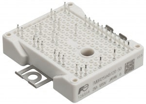
7. What does PIM mean?
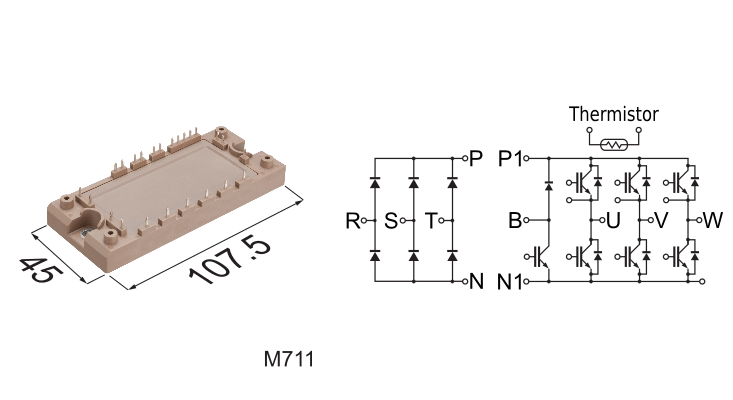
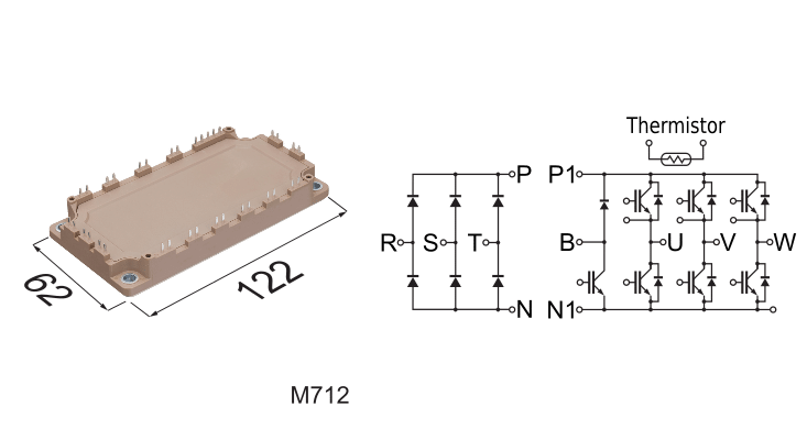
It stands for Power Integrated Module. A PIM is a module that is composed of a 3-phase rectifier circuit, 3-phase inverter circuit, and brake circuit. It is also called CIB (Converter Inverter Brake).
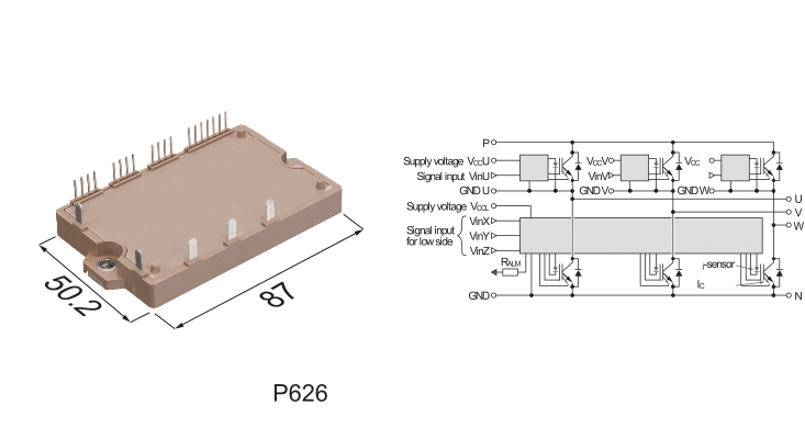
8. What does IPM mean?
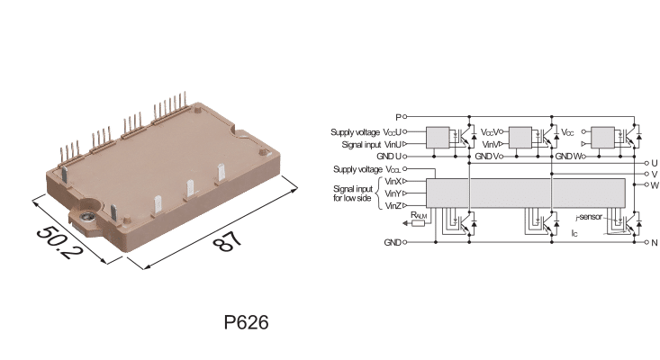
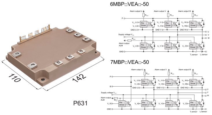
It stands for Intelligent Power Module. An IPM is a module product, based on a 3-phase inverter circuit with a control IC that contains a gate driving circuit and other protection circuits. This product makes it easier to design peripheral circuits than conventional IGBT modules with external driver circuits. The following configurations are possible: 7in1 with a brake circuit, and 6in1 without brake circuit.
9. What is a SiC hybrid module?
This is a product that uses a SiC-SBD (Shottky Barrier Diode) as FWD component, with a combination of Si-IGBT. This combination reduces the losses by approximately 25% in comparison with conventional all-silicon chip products. SiC devices are the focus of attention as next-generation semiconductors that offer superior characteristics in areas such as high withstand-voltage, high-temperature, and high-frequency operations.
10. What is the difference between PIM and IPM?
PIM is a product that integrates a 3-phase converter circuit, brake circuit, and 3-phase inverter circuit into a single module. This leads to a compact main circuit design. IPM, on the other hand, offers an advantage of simple peripheral circuit designing, by use of its built-in control IC. This IC contains gate driving and protection circuits, in addition to brake and inverter circuits.
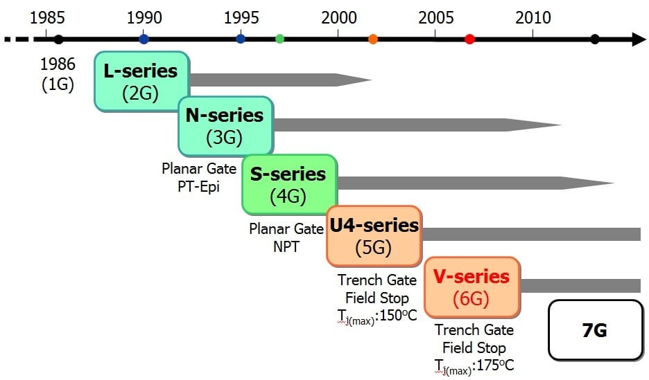
11. What is the V-series of IGBT?
This product series uses our company's 6th-generation IGBT chip set. This chip generation uses a trench gate structure that forms a three-dimensional gate over the silicon surface. It also contains a field stop structure (FS structure) to improve the characteristic of the element withstand voltage. These technologies made it possible to use a thinner silicon wafer which leads to a lower on-voltage, reduced switching losses, and improved switching speed control, compared to Fuji's 5th generation IGBT (U-series IGBT).
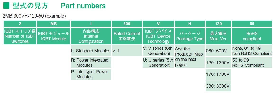
12. How do I read IGBT module model types?
Refer to "Part numbers" in the Semiconductors General Catalog.
13. What is the meaning of each item in the IGBT data sheet?
Refer to the description of terms in Application Manual Chapter 2-1.
14. How do I select a module by the rated parameters?
Regarding voltage and current rating, refer to Application Manual Chapter 3-1 on "how to select an IGBT module". Before use, please verify that the voltage, current, temperature, and other factors stay within the maximum rating range. Please contact Fuji Electric Corp. of America or your local sales representative or distributor for support.
15. Can the voltage exceed IGBT's maximum collector-emitter voltage (VCES) for a short time?
Maximum collector-emitter voltage (VCES) is specified as the maximum rating in the relevant specifications. The voltage should never exceed this value.
16. Is it always expedient to use the gate resistance (RG) value indicated in the data sheet?
The optimum gate resistance value (RG) varies depending on the circuit configuration or operating environment used. The data sheet describes the recommended resistance value to minimize switching loss. Determine an appropriate gate resistance (RG) after considering the relevant switching loss, EMC/EMI, surge voltage, and unexpected characteristics such as vibration, without deviating from the descriptions contained in the data sheet.
17. How should the gate resistance (RG) be determined?
The gate resistance value (RG) greatly impacts dv/dt, radiation noise, voltage/current surge, and switching loss. Please comprehensively determine an appropriate value that corresponds to the target figure of your actual design. As for reference, a recommended turn-on resistance value (RG(on)) is twice or higher than that of the standard value from datasheet, and a recommended turn-off resistance value (RG(off)) is one to two times that of the standard value.
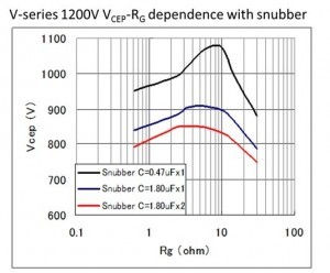
18. How can the surge voltage be reduced?
A surge voltage is generated by high di/dt, and wiring inductance outside the module, at the time of switching (L*di/dt). Some of the ways to suppress this problem are as follows:
(1) Add a protective circuit
(2) Reduce di/dt by adjusting RG or -VGE
(3) Reduce inductance by making the main circuit wiring thicker and shorter, and using a copper bar and parallel flat wiring
For details, refer to Application Manual Chapter 5.
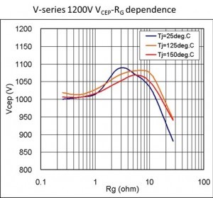
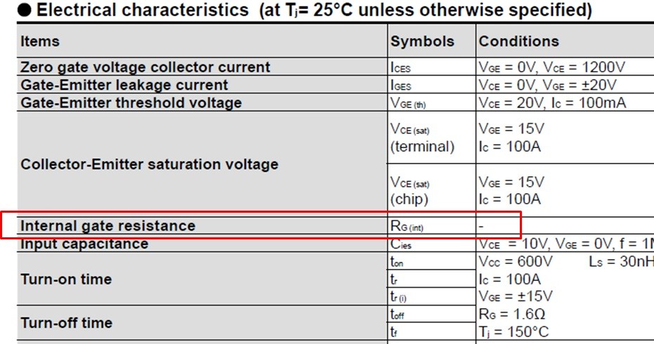
19. What ohm value is set for internal gate resistance (RG) in an IGBT module?
"Refer to the data sheet where internal gate resistance (RG) values for the 6th-generation V-series and 7th-generation X-series IGBT module are described.
Please contact us with a model type number if it is not shown in the 6th-generation data sheet or if it is a product prior to the 6th-generation (U-series, S-series)."
20. What are the points we need to be aware of when determining the gate resistance (RG)?
A larger gate resistance (RG) will increase switching loss, and make it more prone to generating an arm short circuit due to an insufficient dead-time. A smaller gate resistance (RG)may cause a sudden surge voltage. For details, refer to Application Manual Chapters 2-2.2 and 7-1.3.
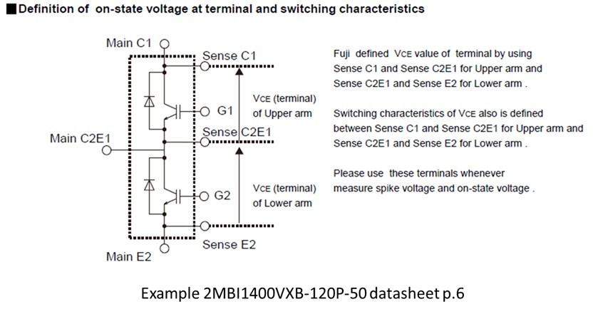
21. Which terminal should be used to measure the collector-emitter voltage (VCE) when switching?
Please measure at the main terminal of the product. If a terminal is separately specified for measurement in the data sheet, please use the specified terminal.
22. What is the reason for applying reverse-bias voltage (-VGE) between the gate and emitter?
An insufficient reverse-bias voltage (-VGE) between the gate and emitter may cause the IGBT to mis-fire, leading to a short-circuit current. If the current is cut off the surge voltage and the generated loss may damage the product. For details, refer to Application Manual Chapters 4-3.3 and 7-1.2.
23. Can application of a reverse-bias voltage (-VGE) on a gate-to-emitter be exempted in a case where only an FWD is used without an opposite IGBT, such as in a chopper circuit?
Please apply a reverse-bias voltage (-VGE) of -5 V or higher (-15 V recommended; max. -20 V) between the gate and emitter in the IGBT that is not being used. An insufficient reverse-bias voltage (-VGE) may cause the IGBT to misfire due to dV/dt at the time of reverse-recovery of the FWD, resulting in damage.
For details, refer to Application Manual Chapter 3-10.
24. What precautions need to be considered when designing an IGBT drive circuit?
Refer to Application Manual Chapter 7-5. It provides precautions regarding the photo-coupler's noise capability, wiring between the drive circuit and IGBT, and gate overvoltage protection.
25. What is the lowest operation temperature for an IGBT module?
The minimum temperature is specified by the storage temperature (Tstg). Please consider that there will be a reduced device withstand voltage and peripheral component (capacitor, control circuit) characteristics under low temperature before use.
26. Can an IPM operate at -40oC?
Our IPM is designed with a lowest guaranteed operating temperature of Tc=-20oC. Operation below this temperature has not been evaluated, and any use below -20oC will void your warranty. At such temperature, there are concerns about possible malfunctions due to a lower device withstand voltage or reduced capacity of the used capacitor.
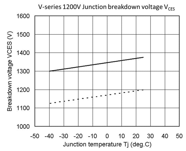
27. Is there a temperature dependency in the IGBT's maximum collector-emitter voltage (VCES)?
A lower temperature reduces the IGBT's maximum collector-emitter voltage (VCES). The data sheet describes the maximum collector-emitter voltage (VCES) under the condition of Tj=25oC. Refer to the technical information describing temperature dependency included in the technical documents under Design Support.
28. How do I calculate IGBT losses?
Fuji provides a free software to calculate the IGBT losses. The following steps can be followed to obtain the figure.
(1) Download our Loss Simulator
(2) Launch our Loss Simulator
(3) Enter data on the chip series, circuit configuration, voltage rating, and current rating. Select your model type. Click ""Next""
(4) Enter data on the circuit, PWM modulation scheme, and calculation conditions. Click ""Calculate""
(5) The calculation result will be displayed
For details, refer to the user manual.
29. What functions do the IGBT Simulator have?
The IGBT Simulator can estimate the power loss and temperature for a 3-phase 2-level inverter circuit, 3-phase 3-level inverter circuit, and chopper circuit of an IGBT and FWD. It can also calculate loss and temperature under variable inverter operation conditions such as output current and switching frequency. Changes in loss and temperature when the load continuously fluctuates, can also be obtained.
30. What is the junction temperature (Tj)?
Junction temperature is the temperature at joints on a semiconductor chip.
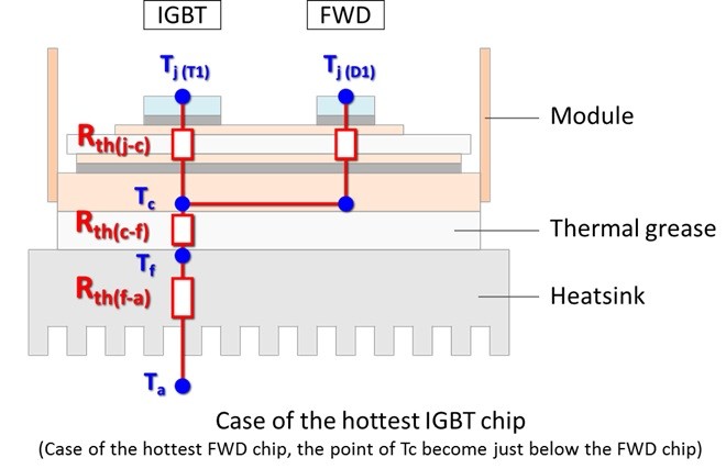
31. What is the case temperature (Tc)?
Case temperature (Tc) is the temperature on the module copper base surface right under a semiconductor chip where the temperature is the highest.
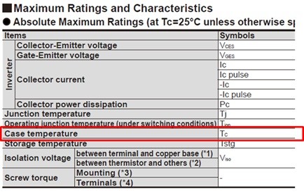
32. What is the acceptable range of case temperature (Tc) for an IGBT module?
Refer to the "Maximum Ratings: Case temperature" section in the data sheet.
33. How do I estimate the junction temperature (Tj)?
Junction temperature can be estimated based on generated losses and thermal resistance Rth(j-c). For details, refer to Application Manual Chapter 6-2.1.
We provide a free software to calculate IGBT's temperature at 2-level inverter, 3-level inverter, and chopper circuits. This software can be downloaded here.
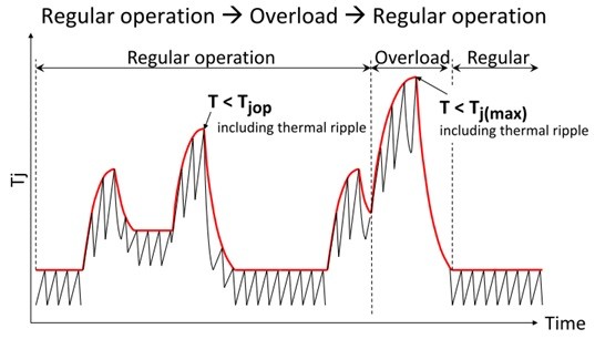
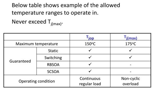
34. What is the difference between Tj(max) and Tj(op)?
The maximum allowable temperature for the chip during conventional continuous operation is specified in Tj(op). Please ensure the maximum chip temperature stays at or under Tj(op) during conventional continuous operation. The maximum allowable temperature for a chip during short-term overload or abnormal operation is specified inTj(max).
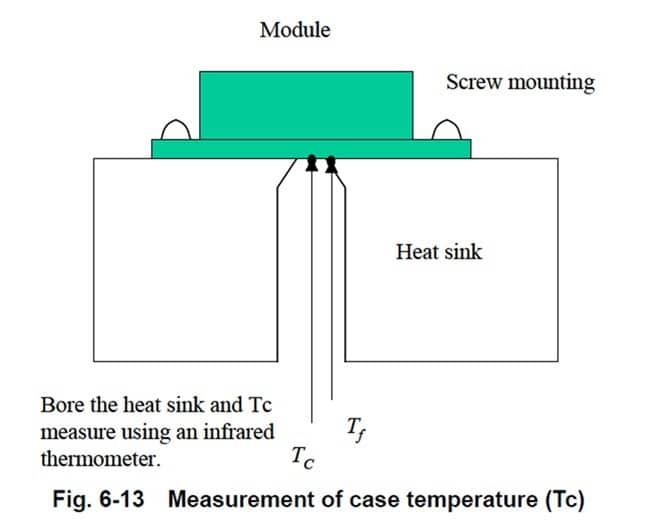
35. How do I measure the case temperature (Tc) for an IGBT module?
The following illustrates an example of how to measure case temperature (Tc).
One method is to make a groove on a copper base or a heat sink of an IGBT module to embed a thermocouple. Please fill the groove with highly thermally conductive paste to secure the thermocouple and attain even thermal diffusion.
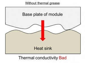
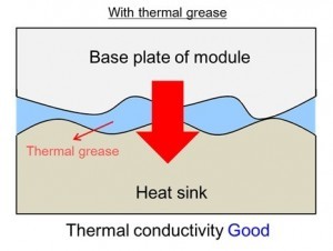
37. Can we apply an IGBT module directly to a heat sink?
No, prior to using an IGBT module, please apply thermal grease (compound) on the surface of a heat sink and module before layering. This will reduce the contact thermal resistance. For details, refer to Application Manual Chapter 6-3.3 or Mounting Instruction.
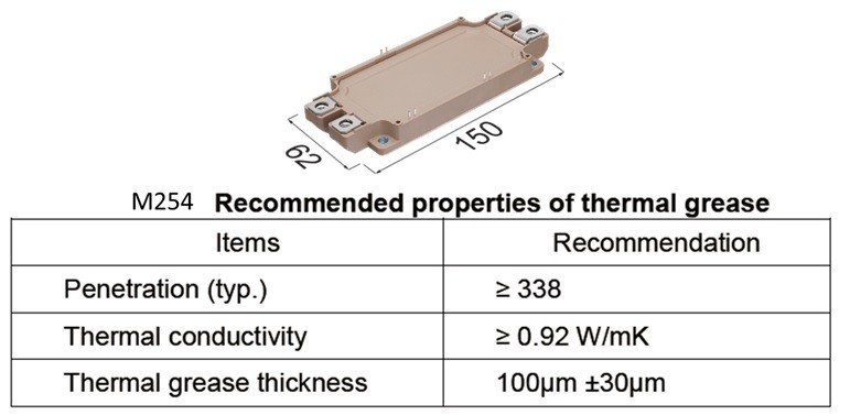
38. What are the recommended thermal conductivity and thickness for thermal grease?
Recommended values are 0.92 W/m·K or higher for thermal conductivity, and approximately 100 μm thick after spreading thermal grease. For details, refer to Application Manual Chapter 6-3.3 or Mounting Instruction.
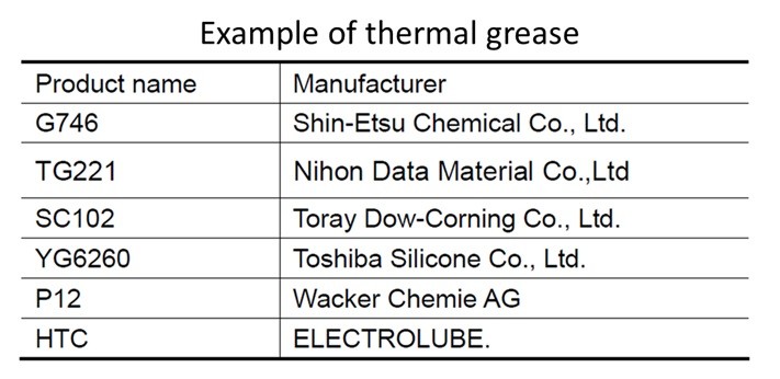
39. Is there a recommended thermal grease that should be used?
Refer to Application Manual Chapter 6-3.3 for details.
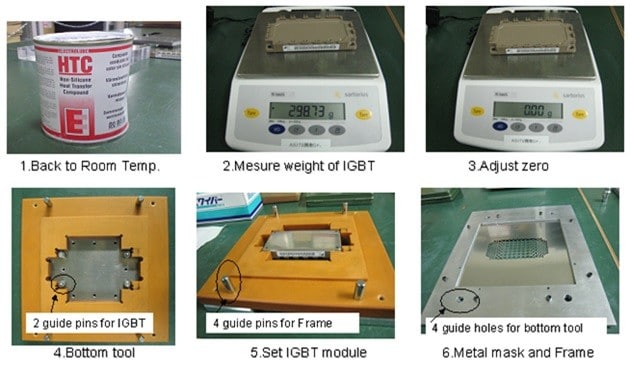
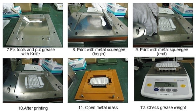
40. How should thermal grease (compound) be applied on an IGBT module?
Thermal grease can be applied using either a roller or stencil mask. An inappropriate thermal grease thickness will negatively affect heat radiation to the heat sink. We strongly recommend using a stencil mask that enables a uniform thickness to be applied over the back surface of the module. For details on application methods, refer to Application Manual Chapter 6-3.3 or Mounting Instruction. An optimum outline drawing for each module is also available. Please contact Fuji Electric Corp. of America or your local sales representative or distributor to answer your question.
41. What thermal grease precautions should we be aware of?
While thermal grease promotes thermal conduction to a fin, it has a thermal capacity itself. Applying too much grease will obstruct the heat radiation to fins. At the same time, applying too little will increase the contact thermal resistance because thermal grease will not have good contact in some spots between the fins and module for bonding. For details, refer to Application Manual Chapter 6-3.3 "Thermal paste application" and technical documents.
42. What range is used for heat sink flatness as a reference?
Guides to flatness values for a heat sink are 50 μm or less for 100 mm between screw mounting locations, and 10 μm or less for surface roughness. An excessive convex warp will cause an insulation breakdown, leading to a critical incident. An excessive concave warp will reduce heat radiation by creating a gap between the product and heat sink, which may lead to thermal destruction.
43. What is a NTC?
NTC (Negative Temperature Coefficient Thermistor) is an electronic component whose resistance decreases while the temperature increases.
44. Is the temperature Tj represented by the NTC temperature?
They are not the same. When incorporating it in an IGBT module, NTC is positioned far from the chip to ensure insulation. This produces a temperature gap between them although NTC's temperature will follow that of chip's Tj.
45. What is the temperature difference between Tj and NTC temperature?
I2t is a Joule-integral for overcurrent allowed within the range that does not result in element destruction. Overcurrent is defined in one cycle at commercially restricted half-waves (50, 60 Hz).
47. What types of power cycle capability are available?
The types of power cycle capability include the ΔTj power cycle (ΔTj-P/C) capability curve and the ΔTc power cycle (ΔTc-P/C) capability curve. We verify device life on two models, therefore please design a product life expectancy within these power cycle capabilities. For details, refer to Application Manual Chapter 11.
48. How do I calculate the power cycle in cases where there are multiple temperature rise peaks?
In cases where the temperature increases n-times per device operation cycle, we assign a power cycle life expectance count as PC(k=1, 2, 3, ..., n). PC(k) is the power cycle life for the k-th temperature rise. A combined power cycle life expectancy count can be expressed by the formula below.
For details, refer to Application Manual Chapter 11.
49. Which parameters have an impact to IGBT's short-circuit current?
IGBT's short-circuit current is impacted by gate-to-emitter voltage VGE, junction temperature Tj, and switching voltage Vcc. Generally, a short-circuit current increases with a large VGE, low Tj, and large Vcc.
50. How can we determine the dead-time?
To prevent a short-circuit in the upper and lower arms, it is necessary to set an on-off timing delay between the several arms. During this time period both devices are switched off. The dead-time needs to be set so that it is generally longer than the switching time of the IGBT (toff max.).
For details, refer to Application Manual Chapter 7.
51. How can we confirm the dead-time?
One way to determine the validity of the dead-time setting is to verify the current on the direct current power line during non-loading time.
For details, refer to Application Manual Chapter 7.
52. Does QG show temperature dependence?
There is no dependency.
53. Does Cies show temperature dependence?
There is no dependency.
54. What types of snubber circuit are available?
There are two types of snubber circuits. The first type is implemented between the DC power supply busbars and is called lump snubber. The second type is called individual snubber ciruit and is connected to each IGBT.
For details, refer to Application Manual Chapter 5.
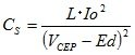
55. How is the capacitor C of the snubber circuit to be determined?
The necessary capacity for a snubber capacitor can be obtained with the following formula.
For details, refer to Application Manual Chapter 5.
56. How do I mount a module?
Refer to IGBT module's Application Manual Chapter 6-3 or Mounting Instruction.
58. What precautions do I need to be aware of when connecting IGBT modules in parallel?
There are four basic precautions, shown below, when connecting IGBT modules in parallel:
(1) Current unbalance control during steady operation
(2) Current unbalance control at the time of switching
(3) Gate drive circuit
(4) Derating
For details, refer to Application Manual Chapter 4-3.5 and Chapter 8.
59. Where are Fuji semiconductor products manufactured?
The semiconductor products of Fuji Electric Corp. of America are manufactured at its six sites in Japan (including Matsumoto Factory, Yamanashi Factory, Fuji Electric Power Semiconductor Co., Ltd., and Fuji Electric Tsugaru Semiconductor Co., Ltd.), and three overseas sites (Fuji Electric (ShenZhen) Co., Ltd., Fuji Electric Philippines, Inc., and Fuji Electric (Malaysia) Sdn. Bhd.).
60. Is there any quality difference between products made in Japan and those made overseas?
Fuji Electric Corp. of America enforces the same quality standard for product management at all locations, regardless of where the manufacturing sites are.
61. Are there any simulation models for the semiconductor products?
A simulation model such as a SPICE model is not available.
62. How do I verify the authenticity of products I have purchased online, etc.?
The desired storage environment has a temperature range of 5 to 35oC, and humidity range of 45% to 75%. Avoid storage under load, and secure a location with little temperature fluctuation. For details, refer to Application Manual Chapter 3-8.
66. What do we need to be aware of when soldering an IGBT module?
67. Are there any measures to prevent misfiring by high dv/dt during the reverse recovery of the FWD?
Some of the ways to prevent misfiring of an IGBT are as follows:
(1) by adding a capacity component CGE to the area between the gate and emitter
(2) by increasing -VGE
(3) by increasing gate resistance (RG)
The effectiveness of these measures will vary depending on the applicable gate circuit, so please verify thoroughly before applying them. For details, refer to Application Manual Chapter 7-1.4.
68. What is the piece of black sponge pinned on the module terminals?
The piece of black sponge is attached for protection. Please keep the sponge on the module at the time of storage.
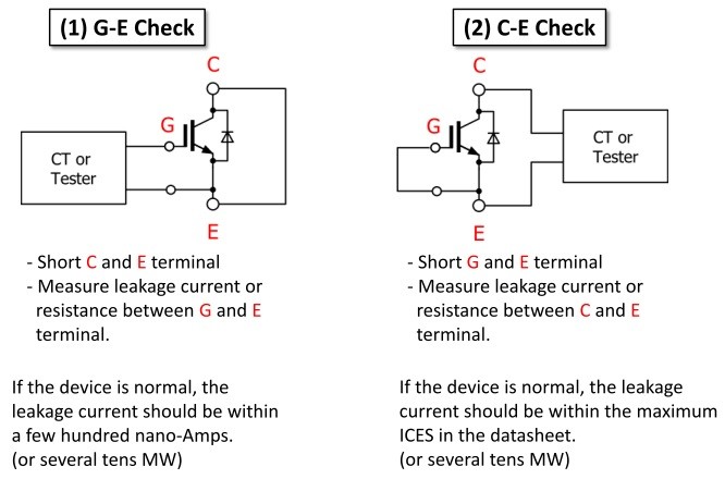
69. Is there any quick way to determine the quality of IGBT before mounting?
You can verify the IGBT by checking the leakage current between G and E, and C and E, using a transistor curve tracer (CT). Simple failure diagnosis can also be done using a voltage, resistance tester in place of a CT. For details, refer to Application Manual Chapter 4-2.
70. What are countermeasures against static electricity when an IGBT module is used?
(1) Discharge any static electricity by grounding through a high-capacity resistor, and use a conductive mat that has been grounded
(2) Hold the package body without directly touching the IGBT module terminals (especially control terminal)
(3) Ground tools such as a soldering tip, at an adequately low resistance
(4) Protect a control terminal using conductive material such as IC foam
For details, refer to Application Manual Chapter 3-2.
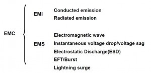
71. What is EMI?
EMI is an abbreviation of Electro Magnetic Interference. The word describes the negative effect caused on peripheral equipment by an electronic device, and it is also called emission. EMI consists of conductive noise that leaks to a power source, and radiation noise that is emitted as electromagnetic waves. For details, refer to Application Manual Chapter 10.
72. What is EMS?
EMS is an abbreviation of Electro Magnetic Susceptibility. The word describes an electronic device's capability and performance against surrounding interference, and it is also called immunity. It includes evaluation items such as electromagnetic waves, static electricity, and lightning surge. For details, refer to Application Manual Chapter 10.
73. How long has Fuji Electric been manufacturing IGBT products?
Fuji Electric Corp. of America began manufacturing IGBTs in 1988, and now has nearly 30 years of history in supplying IGBT products to the market.
74. Is there a lifetime for IGBT modules?
Yes. The main factors impacting the IGBT module's life expectancy are temperature gaps involving the element's junction temperature Tj, and increase and decrease of case temperature Tc. Refer to technical documents describing the relationship of ΔTj and ΔTc with the device life expectancy.
75. How do I read a lot number?
The first digit represents the year of manufacture, the second digit is the month of manufacture, and the remaining 3 to 4 digits are the lot number.
76. How do I handle a terminal when IPM's ALM terminal is not used?
Pull up the ALM terminal to VCC to stabilize electric potential.
77. Where can we obtain an RoHS Certificate of Conformity (CoC)?
79. Have Fuji semiconductor parts an UL certification?
Power semiconductor modules of Fuji Electric Corp. of America have been certified with UL standard 1557, category code QQQX2 (File No. E82988). The relevant model types can be found on the UL website's (http://japan.ul.com/) Online Certifications Directory.
80. How do I handle a terminal when IPM's brake circuit is not used?
Pull up the VinDB terminal to VCC to stabilize electric potential.
81. What is an insulated substrate?
The insulated substrate consists of a ceramic substrate, front-surface copper-foil pattern to create a circuit, and back-surface copper-foil to solder with a copper base. It is designed to electrically insulate between the electric part and the part for thermal dissipation. The ceramic substrate materials used are aluminum oxide, aluminum nitride, silicon nitride, etc.
82. Is there an upper limit of switching frequency for an IGBT?
The switching frequency (carrier frequency) is not defined in specifications. A higher frequency will increase the switching loss, leading to a problem with the junction temperature. The device will be operable under the absolute maximum rated temperature; a frequency of 15 kHz or less should be used for V-series IGBT module. For a welding device or medical equipment it might be necessary to use switching frequencies of 20 kHz or higher, therefore we recommend a high-speed standard 2in1 module or W-series discrete IBGT.
83. Is there any recommended connector for IPM's control terminal?
Connectors compatible with V-IPM series terminal shapes (by HIROSE ELECTRIC CO., LTD.) are on the market. P630: MA49-19S-2.54DSA, MA49-19S-2.54DSA(01)P631: MDF7-25S-2.54DSAPlease contact HIROSE ELECTRIC CO., LTD. to purchase the relevant connector or verify reliability.
84. What type of compatible female terminal (tab terminal) should we choose for a standard package control terminal?
The compatible tab is the 110 series. Please select a tab terminal which has the tab dimensions of 2.8 mm width, and 0.5 mm plate thickness. Relevant products are available on the market from Tyco Electronics Japan G.K., J.S.T. MFG. CO., LTD., and NICHIFU Co., Ltd. Please contact any of these companies for details.
85. What is a press-fit pin?
It is a pin type that allows PCB mounting without soldering. It is used in PIM and 6-Pack products. The time required for the assembly process is reduced as connection is completed by pressing an IGBT module over PCB's through-hole and applying pressure from the base side. Special press and press-in tools are required. We do not sell presses or tools.
86. V-series IPM has VDA and VDN models of the same rating, but what is the difference between them?
VDA and VDN use different material for their insulating substrates, resulting in separate thermal resistance values. The VDA type uses aluminum oxide, while the VDN type uses high heat-radiation material, with approximately 30% less thermal resistance than that of VDA. It is effective when achieving a lower Tj max. or longer ΔTj power cycle life expectancy.
87. What is a bootstrap circuit?
A bootstrap circuit is one that is composed of a control power supply to drive high-side IGBT. It is possible to have a single power supply as it does not require a transformer with multiple secondary windings. Its built-in bootstrap resistance and bootstrap diode (BSD) gives a small IPM to configure a bootstrap circuit simply by adding an external bootstrap capacitor.
88. Is the IPM's input control signal high to switch the IGBT to on?
IPM V-series input control signal is IGBT-on when set at Low. A small IPM's input control signal is IGBT-on when set at High.
89. What factors determine the value of thermal resistance Rth(j-c)?
The thermal resistance value may differ even in the same rating, when comparing different families of products made by Fuji Electric or other companies. A low thermal resistance in a certain product may be due to a larger semiconductor chip size, or the use of a ceramic insulating substrate with good thermal conductivity.
90. The parameter for thermal resistance given in the specification is described as ( per 1 device). What does it mean?
1 device represents a value per arm (IGBT+FWD). Some models connect multiple chips per arm in parallel. This parallel-chip configuration is counted as one chip.
91. What is the meaning of the given gate resistance RG value in the specification? Does this mean external resistance?
It represents an external resistance. It excludes the module's built-in RG(int).
92. What is RBSOA?
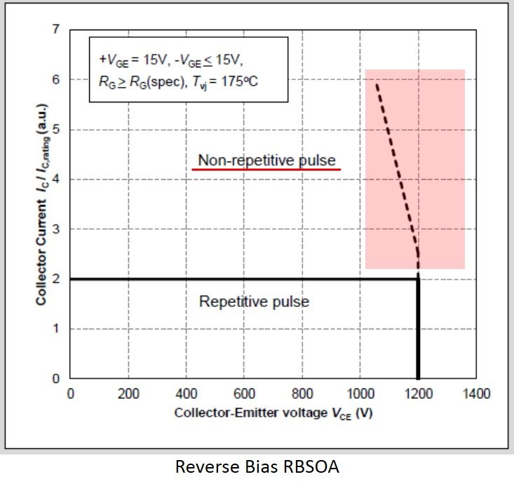
RBSOA is an abbreviation of Reverse Bias Safety Operating Area. The data sheet contains a characteristic graph describing double the rated voltage and rated current under the condition of maximum continuous operation temperature Tj(op). It illustrates a range of VCE and IC where safe operation is maintained when IGBT is turning off. The operation can be repeated within the RBSOA range.
93. What is SCSOA?
SCSOA is an abbreviation of Short Circuit Safety Operating Area. During an incident with an inverter device, such as a load short-circuit, arm short-circuit, or ground fault, a current that is several times higher than the rated current flows in the IGBT. SCSOA is provided to protect the IGBT even during these instances. SCSOA has different characteristics depending on the generation or withstand voltage of IGBT. Refer to the technical documents of individual models.
95. What types of noise are generated at an inverter unit that has a power semiconductor device built in?
There are two types of noise: conductive noise (noise terminal voltage) and radiation noise. Conductive noise propagates over a conductor or earth wire in a main circuit. It is divided into two groups: normal mode and common mode. Radiation noise is generated within a device and emitted into the air because the device wiring or casing works as an antenna. For details, refer to IGBT's Application Manual Chapter 10.
96. How can we reduce conductive noise?
"Conductive noise can be reduced through methods such as adding an LC filter on the AC power side, adding a ferrite core, or adjusting the gate resistance to suppress dv/dt at the time of switching.
For details, refer to IGBT's Application Manual Chapter 10."
97. How can we reduce radiation noise?
Radiation noise can be reduced through methods such as reducing the loop current area where noise is generated, or adjusting the gate resistance. For details, refer to IGBT's Application Manual Chapter 10.
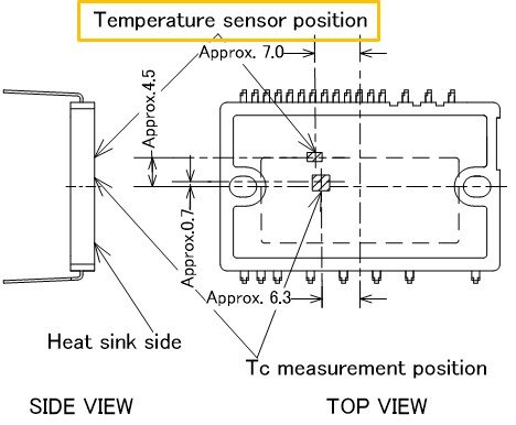
98. Can I get a drawing of the internal chip layout to measure the case temperature TC?
99. How works a stencil mask to apply thermal compound and can I purchase it from Fuji?
A stencil mask is a 200 μm-thick, metal plate with multiple holes punched in the compound application area. A compound can be applied with a uniform thickness of 100 μm when clamping the stencil to a heat sink after application. We do not sell stencil masks but we can provide a mask drawing that corresponds to the relevant package.
100. What happens to IGBT modules in a case where an application exceeds the ΔTj power cycle capability?
It will cause a separation of aluminum wire, or a crack in the solder under the chip. Thermal destruction will result from the current concentrating on the relevant part of the chip, or increased thermal resistance.
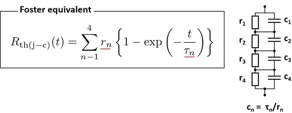
102. How do I use the equation and table that are attached to the transient thermal resistance curve in the data sheet?
The junction temperature Tvj doesn't increase immediately when power losses are generated on a semiconductor chip. There is a time delay due to thermal capacity of materials composing the IGBT module. The equation in the data sheet shows the relationship of the transient thermal resistance to the pulse width tw when a single square wave pulse (power loss) is applied. Transient temperature rise of the junction ΔT(j-c) can be obtained from the transient thermal resistance.
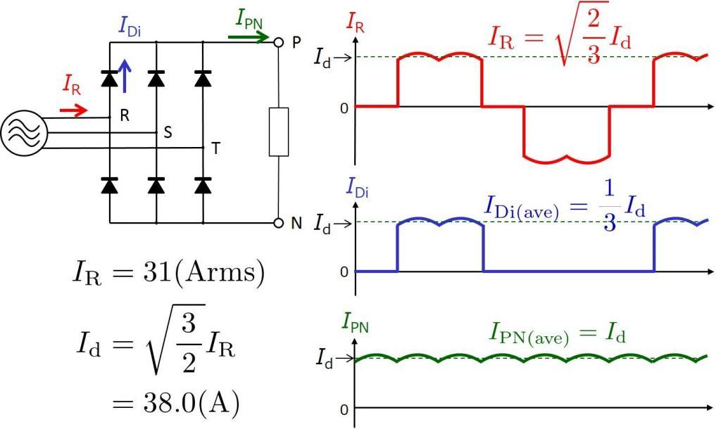
103. There is a converter circuit in the PIM (Power Integrated Module). How to calculate losses of the diode in the converter circuit?
The average value of diode losses in the converter circuit is obtained from the formula below.
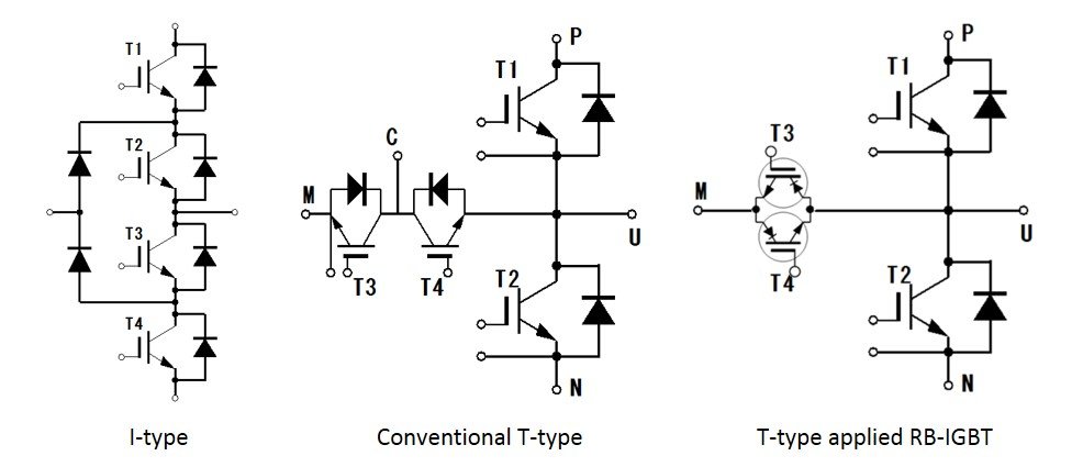
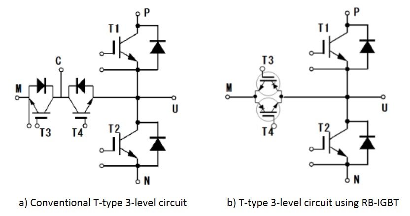
104. What is the difference between an I-type 3-level module and a T-type 3-level module?
Major circuit configurations of 3-level inverters can be categorized in 2 groups, I-type and T-type as shown in the figure below. Fuji Electric has commercialized a T-type which applies two Reverse Blocking IGBTs (RB-IGBT) as a bi-directional switch. The loss can be made smaller compared with the conventional T-type where diode is connected in series with IGBT.
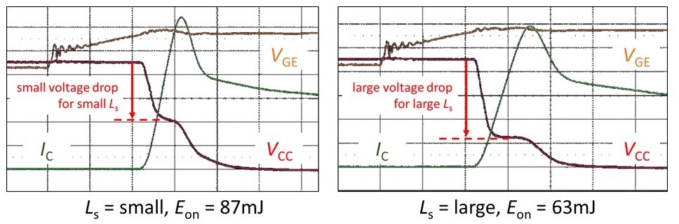
105. What is the influence on the switching loss Eon if the stray inductance Ls of the main circuit is small?
If the stray inductance Ls of the main circuit is small, VCE voltage drop (ΔV=-LSx di/dt) becomes small and Eon becomes large.
106. Can I get dimensions which are not described in the outline drawing included in the data sheet?
107. Can the same thermal grease used for conventional IGBT modules (all-silicon chip) also be used when mounting hybrid SiC modules?
For hybrid SiC modules, the same thermal grease used for conventional all-silicon chip IGBT module can also be used.
108. What are the differences between IPMs (Intelligent Power Modules) types?
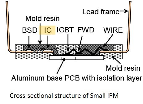
"Fuji has released products with 2500 V isolation voltage (V-IPM, R-IPM) for general industrial application and Small IPMs with 1500 V isolation voltage for air conditioners. The IPMs for general industrial application have a good heat spread characteristic thanks to a copper base plate, and they have protection functions with on chip temperature and current sensors. They are used for servo systems, robots, elevators, etc.
Small IPMs, on the other hand, have a compatible package to other industry-standard package, and offer an advantage of simple peripheral circuit designing thanks to built-in level-shift circuits with high withstand voltage and bootstrap diode."
109. Is it possible to receive the 3D-CAD data of an IGBT module package to design the structure of the main circuit?
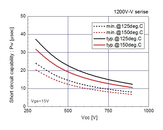
111. Can I get short-circuit withstand capability data?
The short-circuit withstand capability varies with chip generation and withstand voltage. Technical documents that show the relation of the short-circuit withstand capability tSC as a function of DC voltage VCC are available. Please download them from our web site.
112. What is "short-circuit withstand capability"?
In the case of excess current due to an accident or abnormal operation of an inverter device, the time from the start of the short-circuit current until the IGBT breakdown is called the short-circuit withstand capability. The protection circuit has to be designed to detect excess current in a short time not exceeding the short-circuit time and to turn off the gate pulse.
113. What is the maximum current per pin of PIM and 6in1 modules?
For each pin 50 A is the maximum.
114. Is the maximum current per pin the same between solder pins and press-fit pins?
They are the same.
115. What are the selling points of 7th Generation X Series IGBT Modules?
"(1) Low power dissipation
Compared with Fuji's conventional products (the 6th Generation V Series), power loss during inverter operation is reduced by 10%.
(2) Miniaturization
By suppressing heat generation together with power loss reduction, miniaturization of about 36% is achieved compared with conventional products.
(3) High temperature operation and high reliability
Implementation of continuous operation at the maximum junction temperature Tvjop of 175oC, and improvement of reliability.
For details, please refer to 7th Generation IGBT Module "X Series" New Product Information."
116. Why do the currents balance if IGBTs with positive temperature coefficients are connected in parallel?
"Let's consider the case where two IGBTs with different VCEsat are connected in parallel.
(1) A larger amount of the current will flow through the IGBT with smaller VCEsat.
(2) Due to the larger current flow, the total loss of the IGBT becomes large and the junction temperature increase.
(3) If the IGBT has a positive temperature coefficient, VCEsat increases with increasing junction temperature Tvj and hence, the current will decrease until current balance is achieved."
117. Where can we obtain the latest version of data sheets?
121. How do I set up the shunt resistance for excess current detection of a small IPM?
Please refer to Chapter 4.2 of Application Manual.
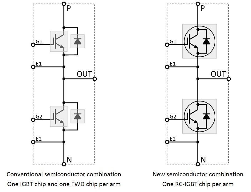
122. What is a RC-IGBT?
RC-IGBT is an acronym of "Reverse Conducting Insulated Gate Bipolar Transistor". The RC chip combines both, IGBT and FWD, in one single chip. It has excellent heat dissipation due to alternating operation of IGBT and FWD as well as reduced number of chips promise miniaturization and high reliability of the IGBT module.
123. What is the dead time?
"To prevent a short-circuit in the upper and lower arms, it is necessary to set an on-off timing delay between the different arms. During the so called 'dead time' period both devices are switched off.
For details, refer to Chapter 7.3 of IGBT Module Application Manual."
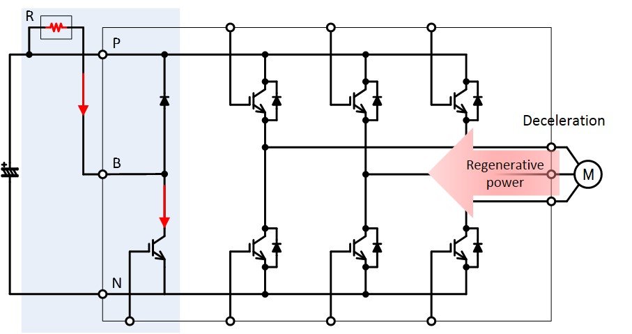
124. What is the function of the brake IGBT, which is part of PIM and IPM?
When a motor stops, the brake IGBT is used to convert kinetic energy of the motor into electric energy and to consume the energy as heat of a resistor (damping resistor). Deceleration time of the motor can be reduced when using a damping resistor. Make sure that the DC voltage does not increase too much with the regenerated energy and exceed the breakdown voltage of the electrolytic capacitor.
125. Is an evaluation board for the IGBT module available?
126. What is the insertion load of the press-fit module?
Please refer to the Mounting Instruction.
127. What is the power cycle capability ΔTc?
Power cycle capability is the capability of the module to withstand repeated heating and cooling. The case temperature Tc will goes up and down until the modules fails: Stress strain is generated between the metal base plate and the insulating substrate causing fatigue in the solder under the insulating substrate. Refer to technical documents describing the relation of ΔTc and the expectancy of life of the device.
128. What is the recommended value of the reverse-bias voltage (-VGE) between gate and emitter?
A range between -5V and -15V is recommended. With lower -VGE, the turn-off time toff becomes large and the turn-off loss Eoff increases. Additionally, the IGBT may misfire and cause a short-circuit current flow.
129. What is the reason of power cycle capability ΔTj curve bending at 50oC?
ΔTj power cycle breakdown mode will become solder degradation mode in the operation with large temperature variation and wire peeling mode in the operation with relatively small temperature variation. Additionally, the transition from plastic to elastic behavior occurs at around 50oC, which causes an inflection point in the curve.
130. What is the relation between switching loss and DC voltage VCC?
They are almost proportional. The switching loss increases as the DC voltage becomes higher.
131. What is the power cycle capability ΔTvj?
In operations where the junction temperature Tvj of a semiconductor chip changes, thermal stress is generated between the materials of the power module. Fatigue will be accumulated from repeated thermal stress, leading to breakdown in the end. Increasing temperature change ΔTvj, leads to a reduction in the lifetime of the power module. It is called as the power cycle capability ΔTvj.
132. The modules with press-fit pins, can they be pulled out and pressed in again?
It is not recommended.
133. The module with press-fit pins, can they be mounted by soldering?
Yes, it is possible.
134. Does a Safety Operating Area for FWD (Free Wheeling Diode) exist?
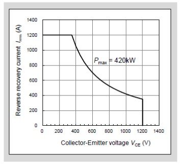
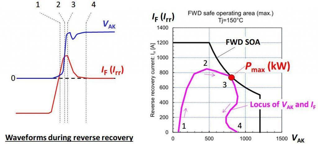
Similar to an IGBT, the FWD has a SOA (Safty Operating Area). Please refer to the following graph which is also shown in the product specifications. It displays an area that indicates the maximum allowed power Pmax. Since Pmax is the product of the voltage VAK applied during reverse recovery and the forward current IF, it limits these two parameters. The design should take into account the SOA and assures that the locus VAK-IF stays within the SOA. If power, exceeding Pmax, is applied, FWD may be damaged. In that case, take countermeasures like increasing the gate resistance of the IGBT ON-side, or using a snubber circuit to suppress the surge voltage.
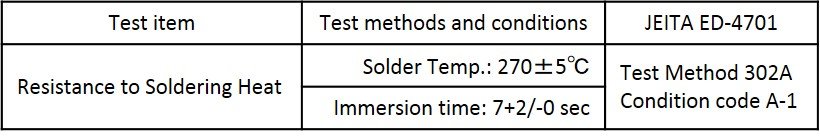
135. What is a recommended soldering condition for the solder pin terminals of IGBT modules?
"Please solder the pins within "Soldering Heat-Resistance Test Conditions" specified in the reliability test items in the specifications.
Please confirm the actual terminal temperature by using a thermocouple."
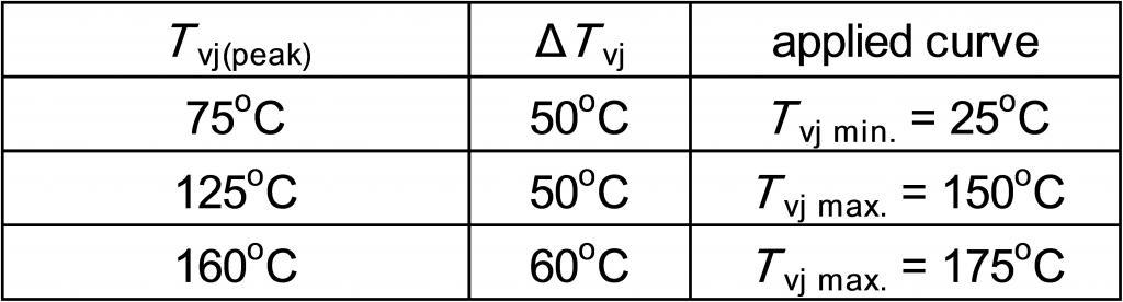
136. Which X Series IGBT module power cycle curves ΔTvj, Tvj min=25oC, Tvj max=150oC and Tvj max=175oC should be used for my design?
These are only exemplary temperatures. If they are not suitable for your application, use the curve that gives the shortest lifetime for your design.
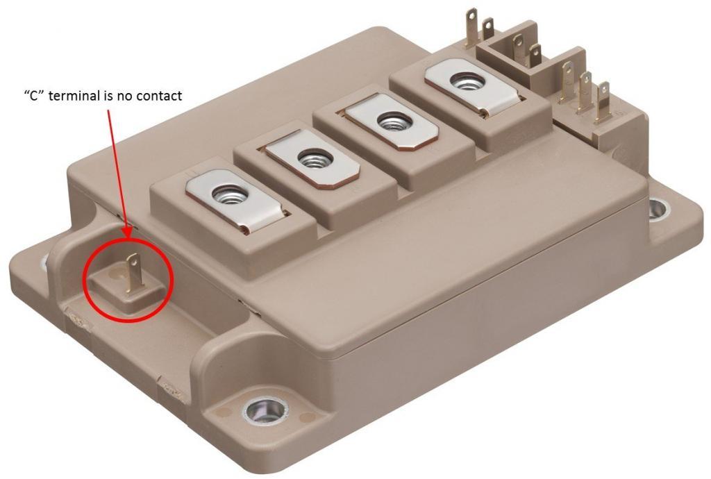
137. The IGBT module for 3-level inverter (Package No.:M403) has an extraordinary terminal. What is the C terminal in the photo used for?
Please do not connect that terminal to anything. It does not have any electrical connection to the IGBT module.
138. We would like to design a DC/DC conversion circuit. Please propose us suitable IGBT modules.
For a voltage boosting circuit, we can offer chopper modules with an IGBT in the low arm side. For step-up/down converter a 2in1 module with 2 IGBTs in series would be suitable. If only one of the two IGBTs is used, please short-circuit gate and emitter of the other one to avoid misfiring.
139. Are 2in1 modules suitable for chopper circuits?
Yes, it is possible to use a 2in1 module in a chopper circuit and use only one of the two IGBTs. To avoid misfiring, please carefully short-circuit gate and the emitter of the unused IGBT.
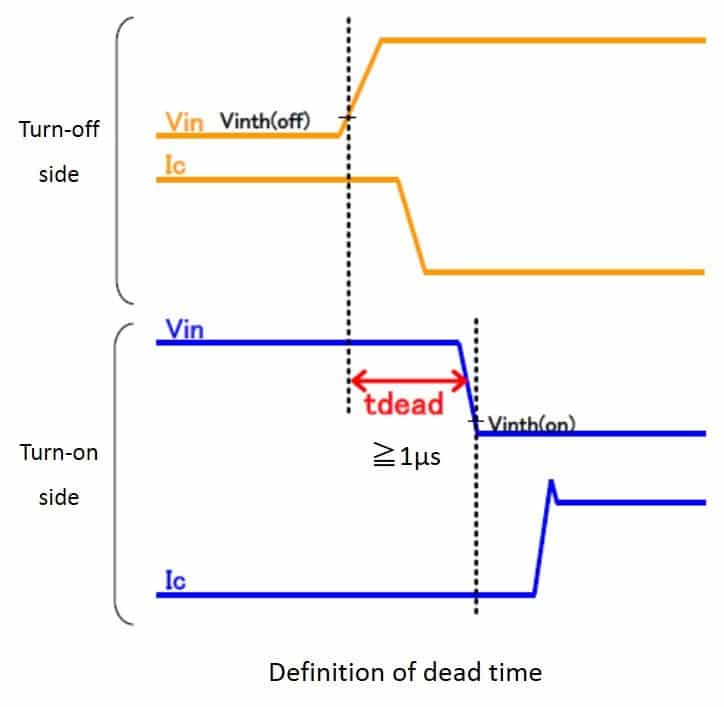
140. The recommended dead time for V-Series IPM is minmum 1μs. Does it indicate the input side (primary side) of a opto-coupler?
No. The dead time indicates the dead time on IPM input terminal Vin.
141. What do I have to take care of when using an IGBT module in a converter circuit?
If diode loss increases, check that the diode temperature does not exceed the absolute maximum ratings, and that ΔTvj power cycle capacity is satisfied. Also check that the system will not be broken due to inrush current at power-on or temporary interruption of power.
142. The alarm output terminal VFO of the small IPM goes to low level when an anomaly occurs within the IPM. What is the alarm output pulse width tFO?
The alarm output period tFO is minimum 20μs, but typical value is about 50μs. The typical value, however, is not guaranteed.
143. What is the successor of the thermal grease G746 (by Shin-Etsu Chemical Co., Ltd) which is recommended in the IGBT Module Application Note?
Fuji recommends the paste 'G776'. Please contact Shin-Etsu Chemical for details. However, Fuji Electric does not guarantee its characteristics when combined with IGBT module.
144. What is the variance of the internal gate resistance (rg) in an IGBT module?
It is ±10%. However, it is not guaranteed.
145. Overheat protection and temperature output functions are built in a small IPM. Which temperature is detected?
The temperature of LVIC (low voltage IC for low arm IGBT drive) is detected. It is not the junction temperature of the IGBT.
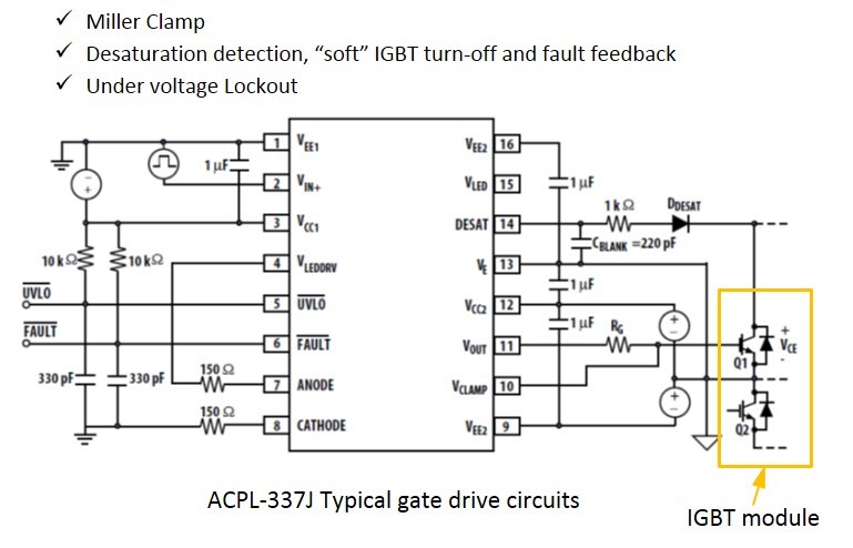
146. Is there any way to simplify the design of the gate drive circuit for the IGBT module and furthermore, include the protection circuit?
IGBT gate drive ICs are supplied from many companies including BROADCOM, Renesas Electronics, Texas Instruments, ISAHAYA ELECTRONICS and TOSHIBA. As the ICs contain short-circuit protection and voltage drop protection circuits within the chip, design of the drive circuit will be simplified. An IGBT module evaluation board with mounted drive IC is available. Please download the information and use it for your reference. However, Fuji Electric does not guarantee its characteristics when combined with an IGBT module.
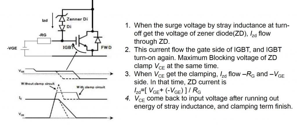
147. What is the active clamp circuit?
It is a protection circuit, added to suppress a surge voltage between the collector and the emitter.
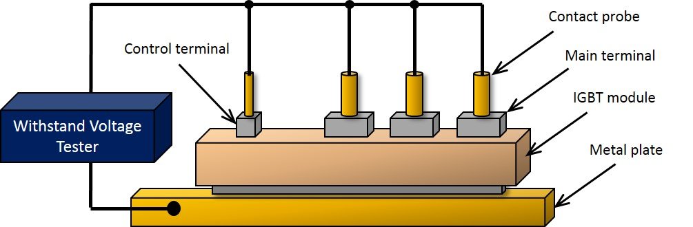
148. What is the insulation voltage test method for IGBT module?
Short-circuit all main and control terminals and apply a specified AC voltage between all terminals and the backside metal area for a specified time period.
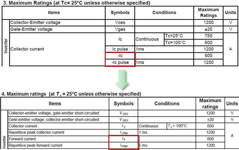
149. -IC, -IC, pulse are included in the absolute maximum ratings. What do they mean?
"Including the V Series, -IC represents the maximum DC forward current which is allowed for the built-in diode, and -Ic, pulse represents the maximum pulse forward current which is allowed for the built-in diode.
From X Series on, to be easily recognized as compliant to IEC standards and as diode elements, they have been changed to IF and IFRM."
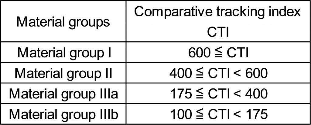
150. What is the CTI (Comparative Tracking Index)?
CTI is the abbreviation for "Comparative Tracking Index".
Those with the comparative tracking index, that indicates tracking resistance as a molding resin, in the material group I in the table are required. The resin molding of power modules used in harsh environment, such as for solar panel generation and wind power generation, improvement in tracking resistance is mandatory.
151. Which snubber capacitors are recommended for modules (M403, M404) used in a 3-level inverter?
There are several snubber capacitors with different withstand voltages and capacitances which meet the main terminal pitch. Please contact RUBYCON CORPORATION.
152. There is a description "package no. M***, P*** in Fuji Electric semiconductor catalog. What does it mean?
"M***: IGBT module product P***: IPM product"
153. Why do I receive the error message "Input value is outside of the setting range." when entering the calculation conditions in the Fuji IGBT loss simulator?
The simulator is based on data obtained by measurement results. The measured values are within the range of representative characteristics described in each data sheet. Input of conditions that are away from actual measurement range will create an error.
154. Does an alarm occur, if the PWM signal is not transmitted to the control input terminal (Vin: High Level) of the V series IPM?
Since the TjOH protection and the UVLO protection are independent from input signals, an alarm signal will be issued when overheat or power supply voltage drop occurs. For Short Circuit (SC) and Over Current (OC) protection will be activated when the input signal is IGBT ON (Vin: Low Level).
155. Once the protection function in Small IPM is triggered and the system stops, how can it be reseted: automatic reset or latch?
It will be reset automatically. After the alarm output period tFO elapsed and the cause of failure has been removed, the protection will reset automatically.
156. VCEsat and VF are given for terminal and chip. How can we use them properly? (What is the meaning?)
"VCEsat and VF of the terminal are ON voltages measured on the main terminals and include voltages induced on the internal wiring of the module. Use them as a reference when On voltage is measured on the terminal.
On the other hand, VCEsat and VF characteristics of the chip indicate IN voltage closest to the semiconductor chip. To obtain the conduction loss that occurs in IGBT and FWD, calculate it from the ON voltage value of the chip."
157. What is the difference between a beige module case and a black module case.
The color is not important from technical point of view. All elder modules including the 5th generation module (U Series) are black. Starting with the 6th generation module (V Series) a natural color (beige) is used to easyly identify the RoHS compliant modules.
158. What are the values of wiring resistance and inductance in the package?
"The resistance of the main current wiring in the module can be calculated from the values of VCEsat and VF of the terminal and the chip shown in the data sheet.
Example: 2MBI600XNE120-50 (Tvj=25oC, Ic=600A) VCEsat (terminal) = 2.20V, VCEsat (chip)=1.45V
Internal wiring resistance Rint = (2.20V-1.45V)/600A=1.25mΩ
Please contact us for the value of internal wiring inductance.
"
159. What is the time dependency of I2t (IFSM)?
Values of I2t and IFSM described in the specification/data sheet shall be the guaranteed value for the half-sine 10ms surge current waveform. For I2t and IFSM for other wavefrom or condition, please contact us.
160. What is the plating material for soldering terminals? (PINS?)
161. Is it possible to adjust the dead time within the IPM?
IPMs do not have a dead time setting function. Please set an adequate dead time in the gate signal input from the outside.
162. Does the value of gate charge QG depends on power supply voltage, current and temperature?
The value of QG does only slightly depend on power supply voltage, current and temperature, hence it is not necessary to consider this dependency in real application.
163. What is the recommended dead time for an IGBT module and an IPM, respectively?
Fuji recommends a dead time larger than 3 μs for IGBT module. For IPMs dead time should be larger than 1 μs.
164. If a pull-down resistor is attached to the temperature output terminal TEMP of small IPM, will the accuracy of the TEMP terminal output voltage change?
The accuracy does not change. The TEMP output voltage shows clamping characteristics at room temperature or below. Please attach a pull-down resistor, if linearity of the output voltage is required for temperatures below room temperature.
165. Is it possible to directly connect the output of the temperature output terminal TEMP of small IPM to the micro processing unit MPU?
The TEMP terminal can directly be connected to the MPU.
166. Is the signal of the temperature output terminal TEMP of small IPM analog or digital?
It is an anolog signal.
167. "What is the difference between E-type and P-type of PrimePACKTM? Example) 2MBI1400VXB-120E-50, 2MBI1400VXB-120P-50"
"In these two different module types different chips are used.
E-type: Standard type
P-type: Soft switching type suppressing turn-off surge voltage"
168. Why does the maximum voltage in the RBSOA (non-repetitive) graph drop when the current is increased?
If the turn-off breaking current increases, di/dt increases as well and is causing an induced electromotive force L·di/dt due to the internal inductance in the module L. Hence, high voltage will be applied to the IGBT chip and might cause some avalanche breakdown. Therefore maximum voltage needs to be reduced when the current increases.
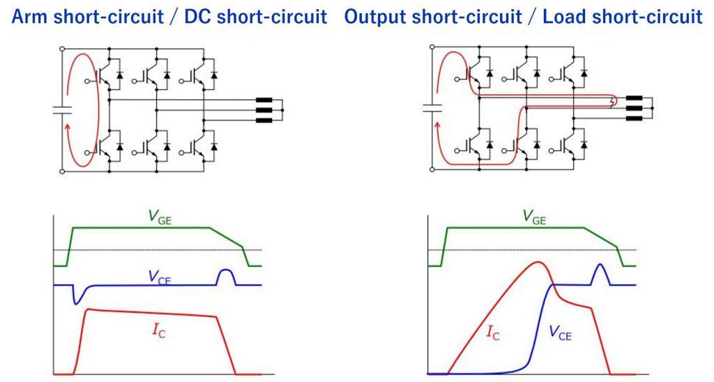
169. What is the difference between DC short circuit (arm short circuit) and load short circuit?
Short circuit withstand capability in the datasheets for our modules are defined in DC short circuit condition (arm short circuit). In the case of load short circuit, the short circuit occurs during conducting mode of the IGBT, and the larger current than the saturation current may flow into the device.
170. Do current IGBT modules still cause a latch-up?
IGBTs developed in recent years are designed to not cause latch-up within a range of normal usage.
171. How can we estimate the IGBT junction temperature from the NTC thermistor built in an IGBT module? What is the heat resistance between the junction temperature and NTC thermistor?
172. Where can I find the description of FBSOA in the IGBT Modules Specifications?
IGBT module do not have a specification of the FBSOA. For IGBT modules the SOA of the FWD is given in the datasheets.
173. Why does Fuji limit the case temperature Topr during operation to -20 -- 110oC for V Series IPM?
IPM contains electronic parts such as PCBs, ICs and capacitors. Therefore, it has a narrower temperature range compared to regular IGBT modules.
174. We like to configure a bootstrap circuit for the upper arm control power supply of a small IPM outside the module as well. Is there any problem?
This is not problematic. Small IPM modules already contain bootstrap diodes and a limiting resistor inside.
175. Why does Fuji recommend to connect a resistor between G-E terminals of IGBT terminal?
If voltage is applied between C-E while the gate is open, the divided voltage by Cres and Cies is applied to the gate, as well. This may lead to a gate breakdown from overvoltage, or a breakdown by heating from elevated device temperature due to a unstable ON state of the gate. As such, for the inverter circuit, the sequence where voltage between C-E is applied after gate circuit is established is recommended. Even if this sequence is not set up, a resistor inserted between G-E to stabilize the gate potential will help to avoid this breakdown phenomenon. In that case, a resistance of about 10kΩ against open (infinite resistance) is recommended. If the resistance is too small, you will see problems such as lower gate voltage than the designed value and an increased current consumption in the drive circuit (because the gate voltage will be the one divided with gate resistance RG.) Therefore, a resistance sufficiently low against the open value is enough and you don’t need to change it according to the current rating of the device.
176. What does Pmax of FWD mean?
The Safe Operation Area (SOA) of a diode indicates the area where the maximum power determined by a product of the current and voltage applied during reverse recovery can be allowed. This maximum power is called as Pmax.
177. When configuring a 3-level converter with T-type, what is the difference between using Fuji Electric orginal RB-IGBT in the AC-switch and using regular IGBT and FWD?
The big benefit of using RB IGBT is that the number of elements that the current goes through is smaller compared with the conventional methods. This leads to a reduction of conductance losses.
178. What is the maximum terminal temperature of the IGBT module?
Its maximum rated terminal temperature is 125oC. However, the allowable maximum terminal temperature of Fuji PrimePACK TM is 150oC.
179. Do all switching losses depend on the gate reverse-bias voltage between the gate and the emitter (-VGE)?
Mainly the turn-off loss Eoff will be affected. As -VGE increases, Eoff decreases.
180. An IGBT module is broken. How can we investigate the cause?
The breakdown mode of an element may include overcurrent, overvoltage, overheat, etc. Causes of each breakdown mode have to be investigated. In the real world, however, it is difficult to identify the cause by the breakdown status of an IGBT module alone. It is important to consolidate information such as the breakdown voltage VCE, current IC, gate voltage VGE, and to make comprehensive investigations. For details, refer to the Application Manual.
181. What are the differences between a 2-level inverter and a 3-level inverter?
A 3-Level inverter realizes system miniaturization and higher efficiency compared to a 2-level inverter. A 2-Level inverter controls the voltage waveform of the converter output with 2 electric potentials while a 3-level inverter controls it with 3 electric potentials. As the 3-level converter creates an output waveform closer to a sinusoidal curve, a reduction of LC filter size and switching loss is expected.
182. After soldering of small IPM products, is it ok to cut their pins off?
There no problem in cutting pins. But please be careful not to apply stress to the PCB.
183. When using an IGBT gate driver IC, do you have any recommended circuits for overcurrent protection?
Follow the recommended circuit for the driver IC. Detemine the circuit constants so that the protection operation will be finished within the period of the short-circuit time indicated for each series.
184. When we apply VGE=15V, is it OK to consider the only range of 15V for SCSOA?
As short-circuit current is determined by the gate voltage, the SCSOA has to be judged by the gate voltage at the time of a short circuit. As the gate voltage may go up in some cases at the time of short circuit, investigation under the worst conditions is recommended.
185. Can we assume that the case surface temperature and the case backside temperature of a discrete IGBT the same?
There is a temperature difference between the surface temperature and the backside temperature. The latter becomes higher.
186. Can we consider that the case temperature Tc is an average value across the copper base plate?
It is not an average value across the copper base plate. It is the case temperature directly under the chip.
187. Can we consider that the case side temperature of an IGBT module is the same as the case temperature Tc?
The case side temperature and the case temperature Tc are different. Heat of a semiconductor chip is conducted through an insulating substrate to the copper base and heatsink. The case side temperature becomes considerably low, compared with Tc.
188. Is the temperature of the NTC thermistor in an IGBT module the same as the case temperature Tc?
The temperature of the NTC thermistor and the case temperature are different. Generally speaking, the case temperature Tc directly under the chip becomes higher than the temperature of the NTC thermistor.
189. Is the temperature of the NTC thermistor in an IGBT module the same as the junction temperature Tvj?
The temperature of the NTC thermistor and the junction temperature Tvj are different. The junction temperature Tvj becomes higher than the temperature of the NTC thermistor. The thermistor is mounted on the same insulating substrate as the IGBT chip but is away from the IGBT chip. It follows the junction temperature Tvj with an offset in time.
190. Is the temperature of the NTC thermistor in an IGBT module the same as the heatsink temperature Ts?
The temperature of the NTC thermistor and the heatsink temperature Ts are different.
191. Are the characteristics of the NTC thermistor built in an IGBT module different depending of the product type? Are there different types for each module?
They are the same. Refer to the Data sheet of each type for resistance value and B constant.
192. Can I use roller and spatula for applying thermal grease to an IGBT module, or is there a problem ?
If roller and/or spatula is used to apply thermal grease, the amount of application may vary or it is impossible to coat the grease evenly. Therefore, those tools are not recommended. Instead, we strongly recommend an application of the grease using stencil masks (See Q40).
193. For thermal calculations of IGBT module, which numeric value should be used, chip or terminal, to estimate/calculate the values of VCEsat and VF?
When you estimate the junction temperature Tvj, please use the chip characteristic data for the calculation.
194. For the V Series IPM a connector, MDF-25S-2.54DSA (by HIROSE ELECTRIC CO., LTD.) is recommended for the high capacity type P631. However, this type has 25 poles which does not match with the IPM control pin count of 16. Do you know a connector with poles extracted from positions where the IPM pin is unavailable?
Please contact HIROSE ELECTRIC. CO., LTD.
195. What are the benefits of a hybrid SiC module?
The benefits are the negligible small diode losses of the SiC diodes. In the following two comparative examples are given for an all-silicon device and a hybrid device with 1200V/300A rating. (1) If both modules have a fixed output current Io=212Arms and the switching frequency of the hybrid module is raised to 1.5 times of the all-silicon one, they still have similar losses. (2) If both modules have a fixed switching frequency fsw=16kHz and the output current of the hybrid module is raised to 1.2 times of the all-silicon device, they still have similar losses.
196. In which applications does Fuji recommend to use hybrid SiC modules?
They are used in industrial inverters, auxiliary inverters for equipment in the Shinkansen cars, high capacity UPS, electric power storage system, etc.
197. Would it be possible to receive ΔTj power cycle lifetime curve for Small IPM?
Yes, it is available on the web site. Please download the data from the link below.
198. Is there any relation between the short-circuit time of the IGBT module tSC and the gate voltage VGE?
Yes. If the gate voltage VGE is high, short-circuit current ISC will increase, and short-circuit withstand time tSC will become shorter.
199. How to calculate the DC-lock in servo drive applications?
The calculation can be done by using the Fuji IGBT Simulator which you find on the webpage.
200. What is the trade-off relation of the IGBT power devices?
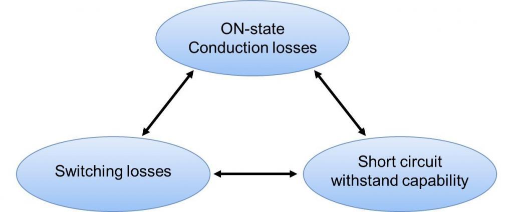
The trade-off relationship of an IGBT describes the relation between ON-state conduction losses, switching losses and short circuit withstand capability. An IGBT can be optimized for either one. For example, when reducing the conduction losses, the switching losses will increase and the short circuit withstand capability decrease.
1. What is an IGBT?
It stands for Insulated Gate Bipolar Transistor. It is a voltage-controlled device that has an insulated gate with an oxide insulating film. The gate structure is similar to a MOSFET. It combines the positive characteristics of a MOSFET and bipolar transistor. It is an indispensable component in a power conversion circuit for high-voltage and large-current applications. It is mainly used in consumer equipment such as air conditioners (a/c) or microwave ovens, industrial equipment such as elevators, and inverters for hybrid electric vehicles (HEV) and electric vehicles (EV).
2. Why is FWD required?
Conventional IGBT elements are not capable of blocking a reverse-withstand voltage. When an inverter circuit is used to drive an inductive load like in a motor, the load current will continue flowing in the reverse direction (emitter to collector) at the time of switching. This may damage the IGBT. The IGBT is protected by a commutating load current in a diode (freewheeling diode: FWD) connected inversely in parallel.
3. What is a RB-IGBT?
It stands for Reverse Blocking Insulated Gate Bipolar Transistor. Reverse-parallel connection of RB-IGBT enables both way switching. It is incorporated in AT-NPC (Advanced T-type Neutral Point Clamped) 3-level inverters, to increase the power conversion efficiency because there are less current passing elements.
4. How do I read IGBT module model types?
Refer to "Part numbers" in the Semiconductors General Catalog.
5. Can the voltage exceed IGBT's maximum collector-emitter voltage (VCES) for a short time?
Maximum collector-emitter voltage (VCES) is specified as the maximum rating in the relevant specifications. The voltage should never exceed this value.
6. What is the junction temperature (Tj)?
Junction temperature is the temperature at joints on a semiconductor chip.
7. What is the case temperature (Tc)?
Case temperature (Tc) is the temperature on the module copper base surface right under a semiconductor chip where the temperature is the highest.
8. Where are Fuji semiconductor products manufactured?
The semiconductor products of Fuji Electric Corp. of America are manufactured at its six sites in Japan (including Matsumoto Factory, Yamanashi Factory, Fuji Electric Power Semiconductor Co., Ltd., and Fuji Electric Tsugaru Semiconductor Co., Ltd.), and three overseas sites (Fuji Electric (ShenZhen) Co., Ltd., Fuji Electric Philippines, Inc., and Fuji Electric (Malaysia) Sdn. Bhd.).
9. Is there any quality difference between products made in Japan and those made overseas?
Fuji Electric Corp. of America enforces the same quality standard for product management at all locations, regardless of where the manufacturing sites are.
10. Is it possible to get a product which is not in the catalog? Does Fuji make customized products?
11. Is there any quick way to determine the quality of IGBT before mounting?
You can verify the IGBT by checking the leakage current between G and E, and C and E, using a transistor curve tracer (CT). Simple failure diagnosis can also be done using a voltage, resistance tester in place of a CT. For details, refer to Application Manual Chapter 4-2.
12. Where can we obtain an RoHS Certificate of Conformity (CoC)?
14. Have Fuji semiconductor parts an UL certification?
Power semiconductor modules of Fuji Electric Corp. of America have been certified with UL standard 1557, category code QQQX2 (File No. E82988). The relevant model types can be found on the UL website's (http://japan.ul.com/) Online Certifications Directory.
15. Is there an upper limit of switching frequency for an IGBT?
The switching frequency (carrier frequency) is not defined in specifications. A higher frequency will increase the switching loss, leading to a problem with the junction temperature. The device will be operable under the absolute maximum rated temperature; a frequency of 15 kHz or less should be used for V-series IGBT module. For a welding device or medical equipment it might be necessary to use switching frequencies of 20 kHz or higher, therefore we recommend a high-speed standard 2in1 module or W-series discrete IBGT.
16. What types of noise are generated at an inverter unit that has a power semiconductor device built in?
There are two types of noise: conductive noise (noise terminal voltage) and radiation noise. Conductive noise propagates over a conductor or earth wire in a main circuit. It is divided into two groups: normal mode and common mode. Radiation noise is generated within a device and emitted into the air because the device wiring or casing works as an antenna. For details, refer to IGBT's Application Manual Chapter 10.
17. How can we reduce conductive noise?
"Conductive noise can be reduced through methods such as adding an LC filter on the AC power side, adding a ferrite core, or adjusting the gate resistance to suppress dv/dt at the time of switching.
For details, refer to IGBT's Application Manual Chapter 10."
18. How can we reduce radiation noise?
Radiation noise can be reduced through methods such as reducing the loop current area where noise is generated, or adjusting the gate resistance. For details, refer to IGBT's Application Manual Chapter 10.
19. Why do the currents balance if IGBTs with positive temperature coefficients are connected in parallel?
"Let's consider the case where two IGBTs with different VCEsat are connected in parallel.
(1) A larger amount of the current will flow through the IGBT with smaller VCEsat.
(2) Due to the larger current flow, the total loss of the IGBT becomes large and the junction temperature increase.
(3) If the IGBT has a positive temperature coefficient, VCEsat increases with increasing junction temperature Tvj and hence, the current will decrease until current balance is achieved."
20. Where can we obtain the latest version of data sheets?
"To prevent a short-circuit in the upper and lower arms, it is necessary to set an on-off timing delay between the different arms. During the so called 'dead time' period both devices are switched off.
For details, refer to Chapter 7.3 of IGBT Module Application Manual."
1. What is an IGBT?
It stands for Insulated Gate Bipolar Transistor. It is a voltage-controlled device that has an insulated gate with an oxide insulating film. The gate structure is similar to a MOSFET. It combines the positive characteristics of a MOSFET and bipolar transistor. It is an indispensable component in a power conversion circuit for high-voltage and large-current applications. It is mainly used in consumer equipment such as air conditioners (a/c) or microwave ovens, industrial equipment such as elevators, and inverters for hybrid electric vehicles (HEV) and electric vehicles (EV).
2. Why is FWD required?
Conventional IGBT elements are not capable of blocking a reverse-withstand voltage. When an inverter circuit is used to drive an inductive load like in a motor, the load current will continue flowing in the reverse direction (emitter to collector) at the time of switching. This may damage the IGBT. The IGBT is protected by a commutating load current in a diode (freewheeling diode: FWD) connected inversely in parallel.
3. What is a RB-IGBT?
It stands for Reverse Blocking Insulated Gate Bipolar Transistor. Reverse-parallel connection of RB-IGBT enables both way switching. It is incorporated in AT-NPC (Advanced T-type Neutral Point Clamped) 3-level inverters, to increase the power conversion efficiency because there are less current passing elements.
4. What is a module?
A module is a package which contains several power semiconductor devices that form a bridge circuit, etc. A modul provides thermal and electrical contact as well as the electrical insulation maintained between the heat-radiation surface and the electric part. For this reason multiple modules can be placed on the same heat sink. Compared to setups that operate with multiple discrete products, the module can handle a larger current and is superior because it is small, lightweight, and easy to assemble.
5. What does PIM mean?
It stands for Power Integrated Module. A PIM is a module that is composed of a 3-phase rectifier circuit, 3-phase inverter circuit, and brake circuit. It is also called CIB (Converter Inverter Brake).
6. What does IPM mean?
It stands for Intelligent Power Module. An IPM is a module product, based on a 3-phase inverter circuit with a control IC that contains a gate driving circuit and other protection circuits. This product makes it easier to design peripheral circuits than conventional IGBT modules with external driver circuits. The following configurations are possible: 7in1 with a brake circuit, and 6in1 without brake circuit.
7. What is a SiC hybrid module?
This is a product that uses a SiC-SBD (Shottky Barrier Diode) as FWD component, with a combination of Si-IGBT. This combination reduces the losses by approximately 25% in comparison with conventional all-silicon chip products. SiC devices are the focus of attention as next-generation semiconductors that offer superior characteristics in areas such as high withstand-voltage, high-temperature, and high-frequency operations.
8. What is the difference between PIM and IPM?
PIM is a product that integrates a 3-phase converter circuit, brake circuit, and 3-phase inverter circuit into a single module. This leads to a compact main circuit design. IPM, on the other hand, offers an advantage of simple peripheral circuit designing, by use of its built-in control IC. This IC contains gate driving and protection circuits, in addition to brake and inverter circuits.
9. What is the V-series of IGBT?
This product series uses our company's 6th-generation IGBT chip set. This chip generation uses a trench gate structure that forms a three-dimensional gate over the silicon surface. It also contains a field stop structure (FS structure) to improve the characteristic of the element withstand voltage. These technologies made it possible to use a thinner silicon wafer which leads to a lower on-voltage, reduced switching losses, and improved switching speed control, compared to Fuji's 5th generation IGBT (U-series IGBT).
10. How do I read IGBT module model types?
Refer to "Part numbers" in the Semiconductors General Catalog.
11. What is the meaning of each item in the IGBT data sheet?
Refer to the description of terms in Application Manual Chapter 2-1.
12. How do I select a module by the rated parameters?
Regarding voltage and current rating, refer to Application Manual Chapter 3-1 on "how to select an IGBT module". Before use, please verify that the voltage, current, temperature, and other factors stay within the maximum rating range. Please contact Fuji Electric Corp. of America or your local sales representative or distributor for support.
13. Can the voltage exceed IGBT's maximum collector-emitter voltage (VCES) for a short time?
Maximum collector-emitter voltage (VCES) is specified as the maximum rating in the relevant specifications. The voltage should never exceed this value.
14. Is it always expedient to use the gate resistance (RG) value indicated in the data sheet?
The optimum gate resistance value (RG) varies depending on the circuit configuration or operating environment used. The data sheet describes the recommended resistance value to minimize switching loss. Determine an appropriate gate resistance (RG) after considering the relevant switching loss, EMC/EMI, surge voltage, and unexpected characteristics such as vibration, without deviating from the descriptions contained in the data sheet.
15. How should the gate resistance (RG) be determined?
The gate resistance value (RG) greatly impacts dv/dt, radiation noise, voltage/current surge, and switching loss. Please comprehensively determine an appropriate value that corresponds to the target figure of your actual design. As for reference, a recommended turn-on resistance value (RG(on)) is twice or higher than that of the standard value from datasheet, and a recommended turn-off resistance value (RG(off)) is one to two times that of the standard value.
16. How can the surge voltage be reduced?
A surge voltage is generated by high di/dt, and wiring inductance outside the module, at the time of switching (L*di/dt). Some of the ways to suppress this problem are as follows:
(1) Add a protective circuit
(2) Reduce di/dt by adjusting RG or -VGE
(3) Reduce inductance by making the main circuit wiring thicker and shorter, and using a copper bar and parallel flat wiring
For details, refer to Application Manual Chapter 5.
17. What ohm value is set for internal gate resistance (RG) in an IGBT module?
"Refer to the data sheet where internal gate resistance (RG) values for the 6th-generation V-series and 7th-generation X-series IGBT module are described.
Please contact us with a model type number if it is not shown in the 6th-generation data sheet or if it is a product prior to the 6th-generation (U-series, S-series)."
18. What are the points we need to be aware of when determining the gate resistance (RG)?
A larger gate resistance (RG) will increase switching loss, and make it more prone to generating an arm short circuit due to an insufficient dead-time. A smaller gate resistance (RG)may cause a sudden surge voltage. For details, refer to Application Manual Chapters 2-2.2 and 7-1.3.
19. Which terminal should be used to measure the collector-emitter voltage (VCE) when switching?
Please measure at the main terminal of the product. If a terminal is separately specified for measurement in the data sheet, please use the specified terminal.
20. What is the reason for applying reverse-bias voltage (-VGE) between the gate and emitter?
An insufficient reverse-bias voltage (-VGE) between the gate and emitter may cause the IGBT to mis-fire, leading to a short-circuit current. If the current is cut off the surge voltage and the generated loss may damage the product. For details, refer to Application Manual Chapters 4-3.3 and 7-1.2.
21. Can application of a reverse-bias voltage (-VGE) on a gate-to-emitter be exempted in a case where only an FWD is used without an opposite IGBT, such as in a chopper circuit?
Please apply a reverse-bias voltage (-VGE) of -5 V or higher (-15 V recommended; max. -20 V) between the gate and emitter in the IGBT that is not being used. An insufficient reverse-bias voltage (-VGE) may cause the IGBT to misfire due to dV/dt at the time of reverse-recovery of the FWD, resulting in damage.
For details, refer to Application Manual Chapter 3-10.
22. What precautions need to be considered when designing an IGBT drive circuit?
Refer to Application Manual Chapter 7-5. It provides precautions regarding the photo-coupler's noise capability, wiring between the drive circuit and IGBT, and gate overvoltage protection.
23. What is the lowest operation temperature for an IGBT module?
The minimum temperature is specified by the storage temperature (Tstg). Please consider that there will be a reduced device withstand voltage and peripheral component (capacitor, control circuit) characteristics under low temperature before use.
24. Can an IPM operate at -40oC?
Our IPM is designed with a lowest guaranteed operating temperature of Tc=-20oC. Operation below this temperature has not been evaluated, and any use below -20oC will void your warranty. At such temperature, there are concerns about possible malfunctions due to a lower device withstand voltage or reduced capacity of the used capacitor.
25. Is there a temperature dependency in the IGBT's maximum collector-emitter voltage (VCES)?
A lower temperature reduces the IGBT's maximum collector-emitter voltage (VCES). The data sheet describes the maximum collector-emitter voltage (VCES) under the condition of Tj=25oC. Refer to the technical information describing temperature dependency included in the technical documents under Design Support.
26. How do I calculate IGBT losses?
Fuji provides a free software to calculate the IGBT losses. The following steps can be followed to obtain the figure.
(1) Download our Loss Simulator
(2) Launch our Loss Simulator
(3) Enter data on the chip series, circuit configuration, voltage rating, and current rating. Select your model type. Click ""Next""
(4) Enter data on the circuit, PWM modulation scheme, and calculation conditions. Click ""Calculate""
(5) The calculation result will be displayed
For details, refer to the user manual.
27. What functions do the IGBT Simulator have?
The IGBT Simulator can estimate the power loss and temperature for a 3-phase 2-level inverter circuit, 3-phase 3-level inverter circuit, and chopper circuit of an IGBT and FWD. It can also calculate loss and temperature under variable inverter operation conditions such as output current and switching frequency. Changes in loss and temperature when the load continuously fluctuates, can also be obtained.
28. What is the junction temperature (Tj)?
Junction temperature is the temperature at joints on a semiconductor chip.
29. What is the case temperature (Tc)?
Case temperature (Tc) is the temperature on the module copper base surface right under a semiconductor chip where the temperature is the highest.
30. What is the acceptable range of case temperature (Tc) for an IGBT module?
Refer to the "Maximum Ratings: Case temperature" section in the data sheet.
31. How do I estimate the junction temperature (Tj)?
Junction temperature can be estimated based on generated losses and thermal resistance Rth(j-c). For details, refer to Application Manual Chapter 6-2.1.
We provide a free software to calculate IGBT's temperature at 2-level inverter, 3-level inverter, and chopper circuits. This software can be downloaded here.
32. What is the difference between Tj(max) and Tj(op)?
The maximum allowable temperature for the chip during conventional continuous operation is specified in Tj(op). Please ensure the maximum chip temperature stays at or under Tj(op) during conventional continuous operation. The maximum allowable temperature for a chip during short-term overload or abnormal operation is specified inTj(max).
33. How do I measure the case temperature (Tc) for an IGBT module?
The following illustrates an example of how to measure case temperature (Tc).
One method is to make a groove on a copper base or a heat sink of an IGBT module to embed a thermocouple. Please fill the groove with highly thermally conductive paste to secure the thermocouple and attain even thermal diffusion.
35. Can we apply an IGBT module directly to a heat sink?
No, prior to using an IGBT module, please apply thermal grease (compound) on the surface of a heat sink and module before layering. This will reduce the contact thermal resistance. For details, refer to Application Manual Chapter 6-3.3 or Mounting Instruction.
36. What are the recommended thermal conductivity and thickness for thermal grease?
Recommended values are 0.92 W/m·K or higher for thermal conductivity, and approximately 100 μm thick after spreading thermal grease. For details, refer to Application Manual Chapter 6-3.3 or Mounting Instruction.
37. Is there a recommended thermal grease that should be used?
Refer to Application Manual Chapter 6-3.3 for details.
38. How should thermal grease (compound) be applied on an IGBT module?
Thermal grease can be applied using either a roller or stencil mask. An inappropriate thermal grease thickness will negatively affect heat radiation to the heat sink. We strongly recommend using a stencil mask that enables a uniform thickness to be applied over the back surface of the module. For details on application methods, refer to Application Manual Chapter 6-3.3 or Mounting Instruction. An optimum outline drawing for each module is also available. Please contact Fuji Electric Corp. of America or your local sales representative or distributor to answer your question.
39. What thermal grease precautions should we be aware of?
While thermal grease promotes thermal conduction to a fin, it has a thermal capacity itself. Applying too much grease will obstruct the heat radiation to fins. At the same time, applying too little will increase the contact thermal resistance because thermal grease will not have good contact in some spots between the fins and module for bonding. For details, refer to Application Manual Chapter 6-3.3 "Thermal paste application" and technical documents.
40. What range is used for heat sink flatness as a reference?
Guides to flatness values for a heat sink are 50 μm or less for 100 mm between screw mounting locations, and 10 μm or less for surface roughness. An excessive convex warp will cause an insulation breakdown, leading to a critical incident. An excessive concave warp will reduce heat radiation by creating a gap between the product and heat sink, which may lead to thermal destruction.
41. What is a NTC?
NTC (Negative Temperature Coefficient Thermistor) is an electronic component whose resistance decreases while the temperature increases.
42. Is the temperature Tj represented by the NTC temperature?
They are not the same. When incorporating it in an IGBT module, NTC is positioned far from the chip to ensure insulation. This produces a temperature gap between them although NTC's temperature will follow that of chip's Tj.
43. What is the temperature difference between Tj and NTC temperature?
I2t is a Joule-integral for overcurrent allowed within the range that does not result in element destruction. Overcurrent is defined in one cycle at commercially restricted half-waves (50, 60 Hz).
45. What types of power cycle capability are available?
The types of power cycle capability include the ΔTj power cycle (ΔTj-P/C) capability curve and the ΔTc power cycle (ΔTc-P/C) capability curve. We verify device life on two models, therefore please design a product life expectancy within these power cycle capabilities. For details, refer to Application Manual Chapter 11.
46. How do I calculate the power cycle in cases where there are multiple temperature rise peaks?
In cases where the temperature increases n-times per device operation cycle, we assign a power cycle life expectance count as PC(k=1, 2, 3, ..., n). PC(k) is the power cycle life for the k-th temperature rise. A combined power cycle life expectancy count can be expressed by the formula below.
For details, refer to Application Manual Chapter 11.
47. Which parameters have an impact to IGBT's short-circuit current?
IGBT's short-circuit current is impacted by gate-to-emitter voltage VGE, junction temperature Tj, and switching voltage Vcc. Generally, a short-circuit current increases with a large VGE, low Tj, and large Vcc.
48. How can we determine the dead-time?
To prevent a short-circuit in the upper and lower arms, it is necessary to set an on-off timing delay between the several arms. During this time period both devices are switched off. The dead-time needs to be set so that it is generally longer than the switching time of the IGBT (toff max.).
For details, refer to Application Manual Chapter 7.
49. How can we confirm the dead-time?
One way to determine the validity of the dead-time setting is to verify the current on the direct current power line during non-loading time.
For details, refer to Application Manual Chapter 7.
50. Does QG show temperature dependence?
There is no dependency.
51. Does Cies show temperature dependence?
There is no dependency.
52. What types of snubber circuit are available?
There are two types of snubber circuits. The first type is implemented between the DC power supply busbars and is called lump snubber. The second type is called individual snubber ciruit and is connected to each IGBT.
For details, refer to Application Manual Chapter 5.
53. How is the capacitor C of the snubber circuit to be determined?
The necessary capacity for a snubber capacitor can be obtained with the following formula.
For details, refer to Application Manual Chapter 5.
54. How do I mount a module?
Refer to IGBT module's Application Manual Chapter 6-3 or Mounting Instruction.
56. What precautions do I need to be aware of when connecting IGBT modules in parallel?
There are four basic precautions, shown below, when connecting IGBT modules in parallel:
(1) Current unbalance control during steady operation
(2) Current unbalance control at the time of switching
(3) Gate drive circuit
(4) Derating
For details, refer to Application Manual Chapter 4-3.5 and Chapter 8.
57. Where are Fuji semiconductor products manufactured?
The semiconductor products of Fuji Electric Corp. of America are manufactured at its six sites in Japan (including Matsumoto Factory, Yamanashi Factory, Fuji Electric Power Semiconductor Co., Ltd., and Fuji Electric Tsugaru Semiconductor Co., Ltd.), and three overseas sites (Fuji Electric (ShenZhen) Co., Ltd., Fuji Electric Philippines, Inc., and Fuji Electric (Malaysia) Sdn. Bhd.).
58. Is there any quality difference between products made in Japan and those made overseas?
Fuji Electric Corp. of America enforces the same quality standard for product management at all locations, regardless of where the manufacturing sites are.
59. Are there any simulation models for the semiconductor products?
A simulation model such as a SPICE model is not available.
60. How do I verify the authenticity of products I have purchased online, etc.?
The desired storage environment has a temperature range of 5 to 35oC, and humidity range of 45% to 75%. Avoid storage under load, and secure a location with little temperature fluctuation. For details, refer to Application Manual Chapter 3-8.
64. What do we need to be aware of when soldering an IGBT module?
65. Are there any measures to prevent misfiring by high dv/dt during the reverse recovery of the FWD?
Some of the ways to prevent misfiring of an IGBT are as follows:
(1) by adding a capacity component CGE to the area between the gate and emitter
(2) by increasing -VGE
(3) by increasing gate resistance (RG)
The effectiveness of these measures will vary depending on the applicable gate circuit, so please verify thoroughly before applying them. For details, refer to Application Manual Chapter 7-1.4.
66. What is the piece of black sponge pinned on the module terminals?
The piece of black sponge is attached for protection. Please keep the sponge on the module at the time of storage.
67. Is there any quick way to determine the quality of IGBT before mounting?
You can verify the IGBT by checking the leakage current between G and E, and C and E, using a transistor curve tracer (CT). Simple failure diagnosis can also be done using a voltage, resistance tester in place of a CT. For details, refer to Application Manual Chapter 4-2.
68. What are countermeasures against static electricity when an IGBT module is used?
(1) Discharge any static electricity by grounding through a high-capacity resistor, and use a conductive mat that has been grounded
(2) Hold the package body without directly touching the IGBT module terminals (especially control terminal)
(3) Ground tools such as a soldering tip, at an adequately low resistance
(4) Protect a control terminal using conductive material such as IC foam
For details, refer to Application Manual Chapter 3-2.
69. What is EMI?
EMI is an abbreviation of Electro Magnetic Interference. The word describes the negative effect caused on peripheral equipment by an electronic device, and it is also called emission. EMI consists of conductive noise that leaks to a power source, and radiation noise that is emitted as electromagnetic waves. For details, refer to Application Manual Chapter 10.
70. What is EMS?
EMS is an abbreviation of Electro Magnetic Susceptibility. The word describes an electronic device's capability and performance against surrounding interference, and it is also called immunity. It includes evaluation items such as electromagnetic waves, static electricity, and lightning surge. For details, refer to Application Manual Chapter 10.
71. How long has Fuji Electric been manufacturing IGBT products?
Fuji Electric Corp. of America began manufacturing IGBTs in 1988, and now has nearly 30 years of history in supplying IGBT products to the market.
72. Is there a lifetime for IGBT modules?
Yes. The main factors impacting the IGBT module's life expectancy are temperature gaps involving the element's junction temperature Tj, and increase and decrease of case temperature Tc. Refer to technical documents describing the relationship of ΔTj and ΔTc with the device life expectancy.
73. How do I read a lot number?
The first digit represents the year of manufacture, the second digit is the month of manufacture, and the remaining 3 to 4 digits are the lot number.
74. How do I handle a terminal when IPM's ALM terminal is not used?
Pull up the ALM terminal to VCC to stabilize electric potential.
75. Where can we obtain an RoHS Certificate of Conformity (CoC)?
77. Have Fuji semiconductor parts an UL certification?
Power semiconductor modules of Fuji Electric Corp. of America have been certified with UL standard 1557, category code QQQX2 (File No. E82988). The relevant model types can be found on the UL website's (http://japan.ul.com/) Online Certifications Directory.
78. How do I handle a terminal when IPM's brake circuit is not used?
Pull up the VinDB terminal to VCC to stabilize electric potential.
79. What is an insulated substrate?
The insulated substrate consists of a ceramic substrate, front-surface copper-foil pattern to create a circuit, and back-surface copper-foil to solder with a copper base. It is designed to electrically insulate between the electric part and the part for thermal dissipation. The ceramic substrate materials used are aluminum oxide, aluminum nitride, silicon nitride, etc.
80. Is there an upper limit of switching frequency for an IGBT?
The switching frequency (carrier frequency) is not defined in specifications. A higher frequency will increase the switching loss, leading to a problem with the junction temperature. The device will be operable under the absolute maximum rated temperature; a frequency of 15 kHz or less should be used for V-series IGBT module. For a welding device or medical equipment it might be necessary to use switching frequencies of 20 kHz or higher, therefore we recommend a high-speed standard 2in1 module or W-series discrete IBGT.
81. Is there any recommended connector for IPM's control terminal?
Connectors compatible with V-IPM series terminal shapes (by HIROSE ELECTRIC CO., LTD.) are on the market. P630: MA49-19S-2.54DSA, MA49-19S-2.54DSA(01)P631: MDF7-25S-2.54DSAPlease contact HIROSE ELECTRIC CO., LTD. to purchase the relevant connector or verify reliability.
82. What type of compatible female terminal (tab terminal) should we choose for a standard package control terminal?
The compatible tab is the 110 series. Please select a tab terminal which has the tab dimensions of 2.8 mm width, and 0.5 mm plate thickness. Relevant products are available on the market from Tyco Electronics Japan G.K., J.S.T. MFG. CO., LTD., and NICHIFU Co., Ltd. Please contact any of these companies for details.
83. What is a press-fit pin?
It is a pin type that allows PCB mounting without soldering. It is used in PIM and 6-Pack products. The time required for the assembly process is reduced as connection is completed by pressing an IGBT module over PCB's through-hole and applying pressure from the base side. Special press and press-in tools are required. We do not sell presses or tools.
84. V-series IPM has VDA and VDN models of the same rating, but what is the difference between them?
VDA and VDN use different material for their insulating substrates, resulting in separate thermal resistance values. The VDA type uses aluminum oxide, while the VDN type uses high heat-radiation material, with approximately 30% less thermal resistance than that of VDA. It is effective when achieving a lower Tj max. or longer ΔTj power cycle life expectancy.
85. What is a bootstrap circuit?
A bootstrap circuit is one that is composed of a control power supply to drive high-side IGBT. It is possible to have a single power supply as it does not require a transformer with multiple secondary windings. Its built-in bootstrap resistance and bootstrap diode (BSD) gives a small IPM to configure a bootstrap circuit simply by adding an external bootstrap capacitor.
86. Is the IPM's input control signal high to switch the IGBT to on?
IPM V-series input control signal is IGBT-on when set at Low. A small IPM's input control signal is IGBT-on when set at High.
87. What factors determine the value of thermal resistance Rth(j-c)?
The thermal resistance value may differ even in the same rating, when comparing different families of products made by Fuji Electric or other companies. A low thermal resistance in a certain product may be due to a larger semiconductor chip size, or the use of a ceramic insulating substrate with good thermal conductivity.
88. The parameter for thermal resistance given in the specification is described as ( per 1 device). What does it mean?
1 device represents a value per arm (IGBT+FWD). Some models connect multiple chips per arm in parallel. This parallel-chip configuration is counted as one chip.
89. What is the meaning of the given gate resistance RG value in the specification? Does this mean external resistance?
It represents an external resistance. It excludes the module's built-in RG(int).
90. What is RBSOA?
RBSOA is an abbreviation of Reverse Bias Safety Operating Area. The data sheet contains a characteristic graph describing double the rated voltage and rated current under the condition of maximum continuous operation temperature Tj(op). It illustrates a range of VCE and IC where safe operation is maintained when IGBT is turning off. The operation can be repeated within the RBSOA range.
91. What is SCSOA?
SCSOA is an abbreviation of Short Circuit Safety Operating Area. During an incident with an inverter device, such as a load short-circuit, arm short-circuit, or ground fault, a current that is several times higher than the rated current flows in the IGBT. SCSOA is provided to protect the IGBT even during these instances. SCSOA has different characteristics depending on the generation or withstand voltage of IGBT. Refer to the technical documents of individual models.
93. What types of noise are generated at an inverter unit that has a power semiconductor device built in?
There are two types of noise: conductive noise (noise terminal voltage) and radiation noise. Conductive noise propagates over a conductor or earth wire in a main circuit. It is divided into two groups: normal mode and common mode. Radiation noise is generated within a device and emitted into the air because the device wiring or casing works as an antenna. For details, refer to IGBT's Application Manual Chapter 10.
94. How can we reduce conductive noise?
"Conductive noise can be reduced through methods such as adding an LC filter on the AC power side, adding a ferrite core, or adjusting the gate resistance to suppress dv/dt at the time of switching.
For details, refer to IGBT's Application Manual Chapter 10."
95. How can we reduce radiation noise?
Radiation noise can be reduced through methods such as reducing the loop current area where noise is generated, or adjusting the gate resistance. For details, refer to IGBT's Application Manual Chapter 10.
96. Can I get a drawing of the internal chip layout to measure the case temperature TC?
97. How works a stencil mask to apply thermal compound and can I purchase it from Fuji?
A stencil mask is a 200 μm-thick, metal plate with multiple holes punched in the compound application area. A compound can be applied with a uniform thickness of 100 μm when clamping the stencil to a heat sink after application. We do not sell stencil masks but we can provide a mask drawing that corresponds to the relevant package.
98. What happens to IGBT modules in a case where an application exceeds the ΔTj power cycle capability?
It will cause a separation of aluminum wire, or a crack in the solder under the chip. Thermal destruction will result from the current concentrating on the relevant part of the chip, or increased thermal resistance.
100. How do I use the equation and table that are attached to the transient thermal resistance curve in the data sheet?
The junction temperature Tvj doesn't increase immediately when power losses are generated on a semiconductor chip. There is a time delay due to thermal capacity of materials composing the IGBT module. The equation in the data sheet shows the relationship of the transient thermal resistance to the pulse width tw when a single square wave pulse (power loss) is applied. Transient temperature rise of the junction ΔT(j-c) can be obtained from the transient thermal resistance.
101. There is a converter circuit in the PIM (Power Integrated Module). How to calculate losses of the diode in the converter circuit?
The average value of diode losses in the converter circuit is obtained from the formula below.
102. What is the difference between an I-type 3-level module and a T-type 3-level module?
Major circuit configurations of 3-level inverters can be categorized in 2 groups, I-type and T-type as shown in the figure below. Fuji Electric has commercialized a T-type which applies two Reverse Blocking IGBTs (RB-IGBT) as a bi-directional switch. The loss can be made smaller compared with the conventional T-type where diode is connected in series with IGBT.
103. What is the influence on the switching loss Eon if the stray inductance Ls of the main circuit is small?
If the stray inductance Ls of the main circuit is small, VCE voltage drop (ΔV=-LSx di/dt) becomes small and Eon becomes large.
104. Can I get dimensions which are not described in the outline drawing included in the data sheet?
105. What are the differences between IPMs (Intelligent Power Modules) types?
"Fuji has released products with 2500 V isolation voltage (V-IPM, R-IPM) for general industrial application and Small IPMs with 1500 V isolation voltage for air conditioners. The IPMs for general industrial application have a good heat spread characteristic thanks to a copper base plate, and they have protection functions with on chip temperature and current sensors. They are used for servo systems, robots, elevators, etc.
Small IPMs, on the other hand, have a compatible package to other industry-standard package, and offer an advantage of simple peripheral circuit designing thanks to built-in level-shift circuits with high withstand voltage and bootstrap diode."
106. Is it possible to receive the 3D-CAD data of an IGBT module package to design the structure of the main circuit?
108. Can I get short-circuit withstand capability data?
The short-circuit withstand capability varies with chip generation and withstand voltage. Technical documents that show the relation of the short-circuit withstand capability tSC as a function of DC voltage VCC are available. Please download them from our web site.
109. What is "short-circuit withstand capability"?
In the case of excess current due to an accident or abnormal operation of an inverter device, the time from the start of the short-circuit current until the IGBT breakdown is called the short-circuit withstand capability. The protection circuit has to be designed to detect excess current in a short time not exceeding the short-circuit time and to turn off the gate pulse.
110. What is the maximum current per pin of PIM and 6in1 modules?
For each pin 50 A is the maximum.
111. Is the maximum current per pin the same between solder pins and press-fit pins?
They are the same.
112. What are the selling points of 7th Generation X Series IGBT Modules?
"(1) Low power dissipation
Compared with Fuji's conventional products (the 6th Generation V Series), power loss during inverter operation is reduced by 10%.
(2) Miniaturization
By suppressing heat generation together with power loss reduction, miniaturization of about 36% is achieved compared with conventional products.
(3) High temperature operation and high reliability
Implementation of continuous operation at the maximum junction temperature Tvjop of 175oC, and improvement of reliability.
For details, please refer to 7th Generation IGBT Module "X Series" New Product Information."
113. Why do the currents balance if IGBTs with positive temperature coefficients are connected in parallel?
"Let's consider the case where two IGBTs with different VCEsat are connected in parallel.
(1) A larger amount of the current will flow through the IGBT with smaller VCEsat.
(2) Due to the larger current flow, the total loss of the IGBT becomes large and the junction temperature increase.
(3) If the IGBT has a positive temperature coefficient, VCEsat increases with increasing junction temperature Tvj and hence, the current will decrease until current balance is achieved."
114. Where can we obtain the latest version of data sheets?
118. How do I set up the shunt resistance for excess current detection of a small IPM?
Please refer to Chapter 4.2 of Application Manual.
119. What is a RC-IGBT?
RC-IGBT is an acronym of "Reverse Conducting Insulated Gate Bipolar Transistor". The RC chip combines both, IGBT and FWD, in one single chip. It has excellent heat dissipation due to alternating operation of IGBT and FWD as well as reduced number of chips promise miniaturization and high reliability of the IGBT module.
120. What is the dead time?
"To prevent a short-circuit in the upper and lower arms, it is necessary to set an on-off timing delay between the different arms. During the so called 'dead time' period both devices are switched off.
For details, refer to Chapter 7.3 of IGBT Module Application Manual."
121. What is the function of the brake IGBT, which is part of PIM and IPM?
When a motor stops, the brake IGBT is used to convert kinetic energy of the motor into electric energy and to consume the energy as heat of a resistor (damping resistor). Deceleration time of the motor can be reduced when using a damping resistor. Make sure that the DC voltage does not increase too much with the regenerated energy and exceed the breakdown voltage of the electrolytic capacitor.
122. Is an evaluation board for the IGBT module available?
123. What is the insertion load of the press-fit module?
Please refer to the Mounting Instruction.
124. What is the power cycle capability ΔTc?
Power cycle capability is the capability of the module to withstand repeated heating and cooling. The case temperature Tc will goes up and down until the modules fails: Stress strain is generated between the metal base plate and the insulating substrate causing fatigue in the solder under the insulating substrate. Refer to technical documents describing the relation of ΔTc and the expectancy of life of the device.
125. What is the recommended value of the reverse-bias voltage (-VGE) between gate and emitter?
A range between -5V and -15V is recommended. With lower -VGE, the turn-off time toff becomes large and the turn-off loss Eoff increases. Additionally, the IGBT may misfire and cause a short-circuit current flow.
126. What is the reason of power cycle capability ΔTj curve bending at 50oC?
ΔTj power cycle breakdown mode will become solder degradation mode in the operation with large temperature variation and wire peeling mode in the operation with relatively small temperature variation. Additionally, the transition from plastic to elastic behavior occurs at around 50oC, which causes an inflection point in the curve.
127. What is the relation between switching loss and DC voltage VCC?
They are almost proportional. The switching loss increases as the DC voltage becomes higher.
128. What is the power cycle capability ΔTvj?
In operations where the junction temperature Tvj of a semiconductor chip changes, thermal stress is generated between the materials of the power module. Fatigue will be accumulated from repeated thermal stress, leading to breakdown in the end. Increasing temperature change ΔTvj, leads to a reduction in the lifetime of the power module. It is called as the power cycle capability ΔTvj.
129. The modules with press-fit pins, can they be pulled out and pressed in again?
It is not recommended.
130. The module with press-fit pins, can they be mounted by soldering?
Yes, it is possible.
131. Does a Safety Operating Area for FWD (Free Wheeling Diode) exist?
Similar to an IGBT, the FWD has a SOA (Safty Operating Area). Please refer to the following graph which is also shown in the product specifications. It displays an area that indicates the maximum allowed power Pmax. Since Pmax is the product of the voltage VAK applied during reverse recovery and the forward current IF, it limits these two parameters. The design should take into account the SOA and assures that the locus VAK-IF stays within the SOA. If power, exceeding Pmax, is applied, FWD may be damaged. In that case, take countermeasures like increasing the gate resistance of the IGBT ON-side, or using a snubber circuit to suppress the surge voltage.
132. What is a recommended soldering condition for the solder pin terminals of IGBT modules?
"Please solder the pins within "Soldering Heat-Resistance Test Conditions" specified in the reliability test items in the specifications.
Please confirm the actual terminal temperature by using a thermocouple."
133. Which X Series IGBT module power cycle curves ΔTvj, Tvj min=25oC, Tvj max=150oC and Tvj max=175oC should be used for my design?
These are only exemplary temperatures. If they are not suitable for your application, use the curve that gives the shortest lifetime for your design.
134. The IGBT module for 3-level inverter (Package No.:M403) has an extraordinary terminal. What is the C terminal in the photo used for?
Please do not connect that terminal to anything. It does not have any electrical connection to the IGBT module.
135. We would like to design a DC/DC conversion circuit. Please propose us suitable IGBT modules.
For a voltage boosting circuit, we can offer chopper modules with an IGBT in the low arm side. For step-up/down converter a 2in1 module with 2 IGBTs in series would be suitable. If only one of the two IGBTs is used, please short-circuit gate and emitter of the other one to avoid misfiring.
136. Are 2in1 modules suitable for chopper circuits?
Yes, it is possible to use a 2in1 module in a chopper circuit and use only one of the two IGBTs. To avoid misfiring, please carefully short-circuit gate and the emitter of the unused IGBT.
137. The recommended dead time for V-Series IPM is minmum 1μs. Does it indicate the input side (primary side) of a opto-coupler?
No. The dead time indicates the dead time on IPM input terminal Vin.
138. What do I have to take care of when using an IGBT module in a converter circuit?
If diode loss increases, check that the diode temperature does not exceed the absolute maximum ratings, and that ΔTvj power cycle capacity is satisfied. Also check that the system will not be broken due to inrush current at power-on or temporary interruption of power.
139. The alarm output terminal VFO of the small IPM goes to low level when an anomaly occurs within the IPM. What is the alarm output pulse width tFO?
The alarm output period tFO is minimum 20μs, but typical value is about 50μs. The typical value, however, is not guaranteed.
140. What is the successor of the thermal grease G746 (by Shin-Etsu Chemical Co., Ltd) which is recommended in the IGBT Module Application Note?
Fuji recommends the paste 'G776'. Please contact Shin-Etsu Chemical for details. However, Fuji Electric does not guarantee its characteristics when combined with IGBT module.
141. What is the variance of the internal gate resistance (rg) in an IGBT module?
It is ±10%. However, it is not guaranteed.
142. Overheat protection and temperature output functions are built in a small IPM. Which temperature is detected?
The temperature of LVIC (low voltage IC for low arm IGBT drive) is detected. It is not the junction temperature of the IGBT.
143. Is there any way to simplify the design of the gate drive circuit for the IGBT module and furthermore, include the protection circuit?
IGBT gate drive ICs are supplied from many companies including BROADCOM, Renesas Electronics, Texas Instruments, ISAHAYA ELECTRONICS and TOSHIBA. As the ICs contain short-circuit protection and voltage drop protection circuits within the chip, design of the drive circuit will be simplified. An IGBT module evaluation board with mounted drive IC is available. Please download the information and use it for your reference. However, Fuji Electric does not guarantee its characteristics when combined with an IGBT module.
144. What is the active clamp circuit?
It is a protection circuit, added to suppress a surge voltage between the collector and the emitter.
145. What is the insulation voltage test method for IGBT module?
Short-circuit all main and control terminals and apply a specified AC voltage between all terminals and the backside metal area for a specified time period.
146. -IC, -IC, pulse are included in the absolute maximum ratings. What do they mean?
"Including the V Series, -IC represents the maximum DC forward current which is allowed for the built-in diode, and -Ic, pulse represents the maximum pulse forward current which is allowed for the built-in diode.
From X Series on, to be easily recognized as compliant to IEC standards and as diode elements, they have been changed to IF and IFRM."
147. What is the CTI (Comparative Tracking Index)?
CTI is the abbreviation for "Comparative Tracking Index".
Those with the comparative tracking index, that indicates tracking resistance as a molding resin, in the material group I in the table are required. The resin molding of power modules used in harsh environment, such as for solar panel generation and wind power generation, improvement in tracking resistance is mandatory.
148. Which snubber capacitors are recommended for modules (M403, M404) used in a 3-level inverter?
There are several snubber capacitors with different withstand voltages and capacitances which meet the main terminal pitch. Please contact RUBYCON CORPORATION.
149. There is a description "package no. M***, P*** in Fuji Electric semiconductor catalog. What does it mean?
"M***: IGBT module product P***: IPM product"
150. Why do I receive the error message "Input value is outside of the setting range." when entering the calculation conditions in the Fuji IGBT loss simulator?
The simulator is based on data obtained by measurement results. The measured values are within the range of representative characteristics described in each data sheet. Input of conditions that are away from actual measurement range will create an error.
151. Does an alarm occur, if the PWM signal is not transmitted to the control input terminal (Vin: High Level) of the V series IPM?
Since the TjOH protection and the UVLO protection are independent from input signals, an alarm signal will be issued when overheat or power supply voltage drop occurs. For Short Circuit (SC) and Over Current (OC) protection will be activated when the input signal is IGBT ON (Vin: Low Level).
152. Once the protection function in Small IPM is triggered and the system stops, how can it be reseted: automatic reset or latch?
It will be reset automatically. After the alarm output period tFO elapsed and the cause of failure has been removed, the protection will reset automatically.
153. VCEsat and VF are given for terminal and chip. How can we use them properly? (What is the meaning?)
"VCEsat and VF of the terminal are ON voltages measured on the main terminals and include voltages induced on the internal wiring of the module. Use them as a reference when On voltage is measured on the terminal.
On the other hand, VCEsat and VF characteristics of the chip indicate IN voltage closest to the semiconductor chip. To obtain the conduction loss that occurs in IGBT and FWD, calculate it from the ON voltage value of the chip."
154. What is the difference between a beige module case and a black module case.
The color is not important from technical point of view. All elder modules including the 5th generation module (U Series) are black. Starting with the 6th generation module (V Series) a natural color (beige) is used to easyly identify the RoHS compliant modules.
155. What are the values of wiring resistance and inductance in the package?
"The resistance of the main current wiring in the module can be calculated from the values of VCEsat and VF of the terminal and the chip shown in the data sheet.
Example: 2MBI600XNE120-50 (Tvj=25oC, Ic=600A) VCEsat (terminal) = 2.20V, VCEsat (chip)=1.45V
Internal wiring resistance Rint = (2.20V-1.45V)/600A=1.25mΩ
Please contact us for the value of internal wiring inductance.
"
156. What is the time dependency of I2t (IFSM)?
Values of I2t and IFSM described in the specification/data sheet shall be the guaranteed value for the half-sine 10ms surge current waveform. For I2t and IFSM for other wavefrom or condition, please contact us.
157. What is the plating material for soldering terminals? (PINS?)
158. Is it possible to adjust the dead time within the IPM?
IPMs do not have a dead time setting function. Please set an adequate dead time in the gate signal input from the outside.
159. Does the value of gate charge QG depends on power supply voltage, current and temperature?
The value of QG does only slightly depend on power supply voltage, current and temperature, hence it is not necessary to consider this dependency in real application.
160. What is the recommended dead time for an IGBT module and an IPM, respectively?
Fuji recommends a dead time larger than 3 μs for IGBT module. For IPMs dead time should be larger than 1 μs.
161. If a pull-down resistor is attached to the temperature output terminal TEMP of small IPM, will the accuracy of the TEMP terminal output voltage change?
The accuracy does not change. The TEMP output voltage shows clamping characteristics at room temperature or below. Please attach a pull-down resistor, if linearity of the output voltage is required for temperatures below room temperature.
162. Is it possible to directly connect the output of the temperature output terminal TEMP of small IPM to the micro processing unit MPU?
The TEMP terminal can directly be connected to the MPU.
163. Is the signal of the temperature output terminal TEMP of small IPM analog or digital?
It is an anolog signal.
164. "What is the difference between E-type and P-type of PrimePACKTM? Example) 2MBI1400VXB-120E-50, 2MBI1400VXB-120P-50"
"In these two different module types different chips are used.
E-type: Standard type
P-type: Soft switching type suppressing turn-off surge voltage"
165. Why does the maximum voltage in the RBSOA (non-repetitive) graph drop when the current is increased?
If the turn-off breaking current increases, di/dt increases as well and is causing an induced electromotive force L·di/dt due to the internal inductance in the module L. Hence, high voltage will be applied to the IGBT chip and might cause some avalanche breakdown. Therefore maximum voltage needs to be reduced when the current increases.
166. What is the difference between DC short circuit (arm short circuit) and load short circuit?
Short circuit withstand capability in the datasheets for our modules are defined in DC short circuit condition (arm short circuit). In the case of load short circuit, the short circuit occurs during conducting mode of the IGBT, and the larger current than the saturation current may flow into the device.
167. Do current IGBT modules still cause a latch-up?
IGBTs developed in recent years are designed to not cause latch-up within a range of normal usage.
168. How can we estimate the IGBT junction temperature from the NTC thermistor built in an IGBT module? What is the heat resistance between the junction temperature and NTC thermistor?
169. Where can I find the description of FBSOA in the IGBT Modules Specifications?
IGBT module do not have a specification of the FBSOA. For IGBT modules the SOA of the FWD is given in the datasheets.
170. Why does Fuji limit the case temperature Topr during operation to -20 -- 110oC for V Series IPM?
IPM contains electronic parts such as PCBs, ICs and capacitors. Therefore, it has a narrower temperature range compared to regular IGBT modules.
171. We like to configure a bootstrap circuit for the upper arm control power supply of a small IPM outside the module as well. Is there any problem?
This is not problematic. Small IPM modules already contain bootstrap diodes and a limiting resistor inside.
172. Why does Fuji recommend to connect a resistor between G-E terminals of IGBT terminal?
If voltage is applied between C-E while the gate is open, the divided voltage by Cres and Cies is applied to the gate, as well. This may lead to a gate breakdown from overvoltage, or a breakdown by heating from elevated device temperature due to a unstable ON state of the gate. As such, for the inverter circuit, the sequence where voltage between C-E is applied after gate circuit is established is recommended. Even if this sequence is not set up, a resistor inserted between G-E to stabilize the gate potential will help to avoid this breakdown phenomenon. In that case, a resistance of about 10kΩ against open (infinite resistance) is recommended. If the resistance is too small, you will see problems such as lower gate voltage than the designed value and an increased current consumption in the drive circuit (because the gate voltage will be the one divided with gate resistance RG.) Therefore, a resistance sufficiently low against the open value is enough and you don’t need to change it according to the current rating of the device.
173. What does Pmax of FWD mean?
The Safe Operation Area (SOA) of a diode indicates the area where the maximum power determined by a product of the current and voltage applied during reverse recovery can be allowed. This maximum power is called as Pmax.
174. When configuring a 3-level converter with T-type, what is the difference between using Fuji Electric orginal RB-IGBT in the AC-switch and using regular IGBT and FWD?
The big benefit of using RB IGBT is that the number of elements that the current goes through is smaller compared with the conventional methods. This leads to a reduction of conductance losses.
175. What is the maximum terminal temperature of the IGBT module?
Its maximum rated terminal temperature is 125oC. However, the allowable maximum terminal temperature of Fuji PrimePACK TM is 150oC.
176. Do all switching losses depend on the gate reverse-bias voltage between the gate and the emitter (-VGE)?
Mainly the turn-off loss Eoff will be affected. As -VGE increases, Eoff decreases.
177. An IGBT module is broken. How can we investigate the cause?
The breakdown mode of an element may include overcurrent, overvoltage, overheat, etc. Causes of each breakdown mode have to be investigated. In the real world, however, it is difficult to identify the cause by the breakdown status of an IGBT module alone. It is important to consolidate information such as the breakdown voltage VCE, current IC, gate voltage VGE, and to make comprehensive investigations. For details, refer to the Application Manual.
178. What are the differences between a 2-level inverter and a 3-level inverter?
A 3-Level inverter realizes system miniaturization and higher efficiency compared to a 2-level inverter. A 2-Level inverter controls the voltage waveform of the converter output with 2 electric potentials while a 3-level inverter controls it with 3 electric potentials. As the 3-level converter creates an output waveform closer to a sinusoidal curve, a reduction of LC filter size and switching loss is expected.
179. After soldering of small IPM products, is it ok to cut their pins off?
There no problem in cutting pins. But please be careful not to apply stress to the PCB.
180. When using an IGBT gate driver IC, do you have any recommended circuits for overcurrent protection?
Follow the recommended circuit for the driver IC. Detemine the circuit constants so that the protection operation will be finished within the period of the short-circuit time indicated for each series.
181. When we apply VGE=15V, is it OK to consider the only range of 15V for SCSOA?
As short-circuit current is determined by the gate voltage, the SCSOA has to be judged by the gate voltage at the time of a short circuit. As the gate voltage may go up in some cases at the time of short circuit, investigation under the worst conditions is recommended.
182. Can we assume that the case surface temperature and the case backside temperature of a discrete IGBT the same?
There is a temperature difference between the surface temperature and the backside temperature. The latter becomes higher.
183. Can we consider that the case temperature Tc is an average value across the copper base plate?
It is not an average value across the copper base plate. It is the case temperature directly under the chip.
184. Can we consider that the case side temperature of an IGBT module is the same as the case temperature Tc?
The case side temperature and the case temperature Tc are different. Heat of a semiconductor chip is conducted through an insulating substrate to the copper base and heatsink. The case side temperature becomes considerably low, compared with Tc.
185. Is the temperature of the NTC thermistor in an IGBT module the same as the case temperature Tc?
The temperature of the NTC thermistor and the case temperature are different. Generally speaking, the case temperature Tc directly under the chip becomes higher than the temperature of the NTC thermistor.
186. Is the temperature of the NTC thermistor in an IGBT module the same as the junction temperature Tvj?
The temperature of the NTC thermistor and the junction temperature Tvj are different. The junction temperature Tvj becomes higher than the temperature of the NTC thermistor. The thermistor is mounted on the same insulating substrate as the IGBT chip but is away from the IGBT chip. It follows the junction temperature Tvj with an offset in time.
187. Is the temperature of the NTC thermistor in an IGBT module the same as the heatsink temperature Ts?
The temperature of the NTC thermistor and the heatsink temperature Ts are different.
188. Are the characteristics of the NTC thermistor built in an IGBT module different depending of the product type? Are there different types for each module?
They are the same. Refer to the Data sheet of each type for resistance value and B constant.
189. Can I use roller and spatula for applying thermal grease to an IGBT module, or is there a problem ?
If roller and/or spatula is used to apply thermal grease, the amount of application may vary or it is impossible to coat the grease evenly. Therefore, those tools are not recommended. Instead, we strongly recommend an application of the grease using stencil masks (See Q40).
190. For thermal calculations of IGBT module, which numeric value should be used, chip or terminal, to estimate/calculate the values of VCEsat and VF?
When you estimate the junction temperature Tvj, please use the chip characteristic data for the calculation.
191. For the V Series IPM a connector, MDF-25S-2.54DSA (by HIROSE ELECTRIC CO., LTD.) is recommended for the high capacity type P631. However, this type has 25 poles which does not match with the IPM control pin count of 16. Do you know a connector with poles extracted from positions where the IPM pin is unavailable?
Please contact HIROSE ELECTRIC. CO., LTD.
192. Would it be possible to receive ΔTj power cycle lifetime curve for Small IPM?
Yes, it is available on the web site. Please download the data from the link below.
193. Is there any relation between the short-circuit time of the IGBT module tSC and the gate voltage VGE?
Yes. If the gate voltage VGE is high, short-circuit current ISC will increase, and short-circuit withstand time tSC will become shorter.
194. How to calculate the DC-lock in servo drive applications?
The calculation can be done by using the Fuji IGBT Simulator which you find on the webpage.
195. What is the trade-off relation of the IGBT power devices?
The trade-off relationship of an IGBT describes the relation between ON-state conduction losses, switching losses and short circuit withstand capability. An IGBT can be optimized for either one. For example, when reducing the conduction losses, the switching losses will increase and the short circuit withstand capability decrease.
1. Where are Fuji semiconductor products manufactured?
The semiconductor products of Fuji Electric Corp. of America are manufactured at its six sites in Japan (including Matsumoto Factory, Yamanashi Factory, Fuji Electric Power Semiconductor Co., Ltd., and Fuji Electric Tsugaru Semiconductor Co., Ltd.), and three overseas sites (Fuji Electric (ShenZhen) Co., Ltd., Fuji Electric Philippines, Inc., and Fuji Electric (Malaysia) Sdn. Bhd.).
2. Is there any quality difference between products made in Japan and those made overseas?
Fuji Electric Corp. of America enforces the same quality standard for product management at all locations, regardless of where the manufacturing sites are.
3. Is it possible to get a product which is not in the catalog? Does Fuji make customized products?
6. Have Fuji semiconductor parts an UL certification?
Power semiconductor modules of Fuji Electric Corp. of America have been certified with UL standard 1557, category code QQQX2 (File No. E82988). The relevant model types can be found on the UL website's (http://japan.ul.com/) Online Certifications Directory.
7. Where can we obtain the latest version of data sheets?
1. What is the difference between an IGBT and a MOSFET?
An IGBT is a device that has a basic structure of a P-layer added to the drain side of a MOSFET. An IGBT is suited for large-current and high withstand-voltage applications. A MOSFET is suited for small-capacity and high-speed switching applications.
2. What is the junction temperature (Tj)?
Junction temperature is the temperature at joints on a semiconductor chip.
3. What is the case temperature (Tc)?
Case temperature (Tc) is the temperature on the module copper base surface right under a semiconductor chip where the temperature is the highest.
4. Where are Fuji semiconductor products manufactured?
The semiconductor products of Fuji Electric Corp. of America are manufactured at its six sites in Japan (including Matsumoto Factory, Yamanashi Factory, Fuji Electric Power Semiconductor Co., Ltd., and Fuji Electric Tsugaru Semiconductor Co., Ltd.), and three overseas sites (Fuji Electric (ShenZhen) Co., Ltd., Fuji Electric Philippines, Inc., and Fuji Electric (Malaysia) Sdn. Bhd.).
5. Is there any quality difference between products made in Japan and those made overseas?
Fuji Electric Corp. of America enforces the same quality standard for product management at all locations, regardless of where the manufacturing sites are.
6. Is it possible to get a product which is not in the catalog? Does Fuji make customized products?
7. Is there any quick way to determine the quality of IGBT before mounting?
You can verify the IGBT by checking the leakage current between G and E, and C and E, using a transistor curve tracer (CT). Simple failure diagnosis can also be done using a voltage, resistance tester in place of a CT. For details, refer to Application Manual Chapter 4-2.
8. Where can we obtain an RoHS Certificate of Conformity (CoC)?
10. Have Fuji semiconductor parts an UL certification?
Power semiconductor modules of Fuji Electric Corp. of America have been certified with UL standard 1557, category code QQQX2 (File No. E82988). The relevant model types can be found on the UL website's (http://japan.ul.com/) Online Certifications Directory.
11. What types of noise are generated at an inverter unit that has a power semiconductor device built in?
There are two types of noise: conductive noise (noise terminal voltage) and radiation noise. Conductive noise propagates over a conductor or earth wire in a main circuit. It is divided into two groups: normal mode and common mode. Radiation noise is generated within a device and emitted into the air because the device wiring or casing works as an antenna. For details, refer to IGBT's Application Manual Chapter 10.
12. How can we reduce conductive noise?
"Conductive noise can be reduced through methods such as adding an LC filter on the AC power side, adding a ferrite core, or adjusting the gate resistance to suppress dv/dt at the time of switching.
For details, refer to IGBT's Application Manual Chapter 10."
13. How can we reduce radiation noise?
Radiation noise can be reduced through methods such as reducing the loop current area where noise is generated, or adjusting the gate resistance. For details, refer to IGBT's Application Manual Chapter 10.
14. Why do the currents balance if IGBTs with positive temperature coefficients are connected in parallel?
"Let's consider the case where two IGBTs with different VCEsat are connected in parallel.
(1) A larger amount of the current will flow through the IGBT with smaller VCEsat.
(2) Due to the larger current flow, the total loss of the IGBT becomes large and the junction temperature increase.
(3) If the IGBT has a positive temperature coefficient, VCEsat increases with increasing junction temperature Tvj and hence, the current will decrease until current balance is achieved."
15. Where can we obtain the latest version of data sheets?
"To prevent a short-circuit in the upper and lower arms, it is necessary to set an on-off timing delay between the different arms. During the so called 'dead time' period both devices are switched off.
For details, refer to Chapter 7.3 of IGBT Module Application Manual."
1. What is the junction temperature (Tj)?
Junction temperature is the temperature at joints on a semiconductor chip.
2. What is the case temperature (Tc)?
Case temperature (Tc) is the temperature on the module copper base surface right under a semiconductor chip where the temperature is the highest.
3. What is the diode's I2t?
I2t is a Joule-integral for overcurrent allowed within the range that does not result in element destruction. Overcurrent is defined in one cycle at commercially restricted half-waves (50, 60 Hz).
4. Where are Fuji semiconductor products manufactured?
The semiconductor products of Fuji Electric Corp. of America are manufactured at its six sites in Japan (including Matsumoto Factory, Yamanashi Factory, Fuji Electric Power Semiconductor Co., Ltd., and Fuji Electric Tsugaru Semiconductor Co., Ltd.), and three overseas sites (Fuji Electric (ShenZhen) Co., Ltd., Fuji Electric Philippines, Inc., and Fuji Electric (Malaysia) Sdn. Bhd.).
5. Is there any quality difference between products made in Japan and those made overseas?
Fuji Electric Corp. of America enforces the same quality standard for product management at all locations, regardless of where the manufacturing sites are.
6. Is it possible to get a product which is not in the catalog? Does Fuji make customized products?
9. Have Fuji semiconductor parts an UL certification?
Power semiconductor modules of Fuji Electric Corp. of America have been certified with UL standard 1557, category code QQQX2 (File No. E82988). The relevant model types can be found on the UL website's (http://japan.ul.com/) Online Certifications Directory.
10. What types of noise are generated at an inverter unit that has a power semiconductor device built in?
There are two types of noise: conductive noise (noise terminal voltage) and radiation noise. Conductive noise propagates over a conductor or earth wire in a main circuit. It is divided into two groups: normal mode and common mode. Radiation noise is generated within a device and emitted into the air because the device wiring or casing works as an antenna. For details, refer to IGBT's Application Manual Chapter 10.
11. How can we reduce conductive noise?
"Conductive noise can be reduced through methods such as adding an LC filter on the AC power side, adding a ferrite core, or adjusting the gate resistance to suppress dv/dt at the time of switching.
For details, refer to IGBT's Application Manual Chapter 10."
12. How can we reduce radiation noise?
Radiation noise can be reduced through methods such as reducing the loop current area where noise is generated, or adjusting the gate resistance. For details, refer to IGBT's Application Manual Chapter 10.
13. Where can we obtain the latest version of data sheets?
It stands for Insulated Gate Bipolar Transistor. It is a voltage-controlled device that has an insulated gate with an oxide insulating film. The gate structure is similar to a MOSFET. It combines the positive characteristics of a MOSFET and bipolar transistor. It is an indispensable component in a power conversion circuit for high-voltage and large-current applications. It is mainly used in consumer equipment such as air conditioners (a/c) or microwave ovens, industrial equipment such as elevators, and inverters for hybrid electric vehicles (HEV) and electric vehicles (EV).
2. Why is FWD required?
Conventional IGBT elements are not capable of blocking a reverse-withstand voltage. When an inverter circuit is used to drive an inductive load like in a motor, the load current will continue flowing in the reverse direction (emitter to collector) at the time of switching. This may damage the IGBT. The IGBT is protected by a commutating load current in a diode (freewheeling diode: FWD) connected inversely in parallel.
3. What is the difference between an IGBT and a MOSFET?
An IGBT is a device that has a basic structure of a P-layer added to the drain side of a MOSFET. An IGBT is suited for large-current and high withstand-voltage applications. A MOSFET is suited for small-capacity and high-speed switching applications.
4. What does SiC mean?
It stands for Silicon Carbide. SiC has a wider bandgap width compared to silicon, and is expected to become the next-generation power device material for high-temperature operation, high-speed switching, low power-loss, and high withstand-voltage applications.
5. What is a module?
A module is a package which contains several power semiconductor devices that form a bridge circuit, etc. A modul provides thermal and electrical contact as well as the electrical insulation maintained between the heat-radiation surface and the electric part. For this reason multiple modules can be placed on the same heat sink. Compared to setups that operate with multiple discrete products, the module can handle a larger current and is superior because it is small, lightweight, and easy to assemble.
6. What does PIM mean?
It stands for Power Integrated Module. A PIM is a module that is composed of a 3-phase rectifier circuit, 3-phase inverter circuit, and brake circuit. It is also called CIB (Converter Inverter Brake).
7. What is a SiC hybrid module?
This is a product that uses a SiC-SBD (Shottky Barrier Diode) as FWD component, with a combination of Si-IGBT. This combination reduces the losses by approximately 25% in comparison with conventional all-silicon chip products. SiC devices are the focus of attention as next-generation semiconductors that offer superior characteristics in areas such as high withstand-voltage, high-temperature, and high-frequency operations.
8. What is the difference between PIM and IPM?
PIM is a product that integrates a 3-phase converter circuit, brake circuit, and 3-phase inverter circuit into a single module. This leads to a compact main circuit design. IPM, on the other hand, offers an advantage of simple peripheral circuit designing, by use of its built-in control IC. This IC contains gate driving and protection circuits, in addition to brake and inverter circuits.
9. How do I read IGBT module model types?
Refer to "Part numbers" in the Semiconductors General Catalog.
10. What is the meaning of each item in the IGBT data sheet?
Refer to the description of terms in Application Manual Chapter 2-1.
11. How do I select a module by the rated parameters?
Regarding voltage and current rating, refer to Application Manual Chapter 3-1 on "how to select an IGBT module". Before use, please verify that the voltage, current, temperature, and other factors stay within the maximum rating range. Please contact Fuji Electric Corp. of America or your local sales representative or distributor for support.
12. Can the voltage exceed IGBT's maximum collector-emitter voltage (VCES) for a short time?
Maximum collector-emitter voltage (VCES) is specified as the maximum rating in the relevant specifications. The voltage should never exceed this value.
13. Is it always expedient to use the gate resistance (RG) value indicated in the data sheet?
The optimum gate resistance value (RG) varies depending on the circuit configuration or operating environment used. The data sheet describes the recommended resistance value to minimize switching loss. Determine an appropriate gate resistance (RG) after considering the relevant switching loss, EMC/EMI, surge voltage, and unexpected characteristics such as vibration, without deviating from the descriptions contained in the data sheet.
14. How should the gate resistance (RG) be determined?
The gate resistance value (RG) greatly impacts dv/dt, radiation noise, voltage/current surge, and switching loss. Please comprehensively determine an appropriate value that corresponds to the target figure of your actual design. As for reference, a recommended turn-on resistance value (RG(on)) is twice or higher than that of the standard value from datasheet, and a recommended turn-off resistance value (RG(off)) is one to two times that of the standard value.
15. How can the surge voltage be reduced?
A surge voltage is generated by high di/dt, and wiring inductance outside the module, at the time of switching (L*di/dt). Some of the ways to suppress this problem are as follows:
(1) Add a protective circuit
(2) Reduce di/dt by adjusting RG or -VGE
(3) Reduce inductance by making the main circuit wiring thicker and shorter, and using a copper bar and parallel flat wiring
For details, refer to Application Manual Chapter 5.
16. What are the points we need to be aware of when determining the gate resistance (RG)?
A larger gate resistance (RG) will increase switching loss, and make it more prone to generating an arm short circuit due to an insufficient dead-time. A smaller gate resistance (RG)may cause a sudden surge voltage. For details, refer to Application Manual Chapters 2-2.2 and 7-1.3.
17. Which terminal should be used to measure the collector-emitter voltage (VCE) when switching?
Please measure at the main terminal of the product. If a terminal is separately specified for measurement in the data sheet, please use the specified terminal.
18. What is the reason for applying reverse-bias voltage (-VGE) between the gate and emitter?
An insufficient reverse-bias voltage (-VGE) between the gate and emitter may cause the IGBT to mis-fire, leading to a short-circuit current. If the current is cut off the surge voltage and the generated loss may damage the product. For details, refer to Application Manual Chapters 4-3.3 and 7-1.2.
19. Can application of a reverse-bias voltage (-VGE) on a gate-to-emitter be exempted in a case where only an FWD is used without an opposite IGBT, such as in a chopper circuit?
Please apply a reverse-bias voltage (-VGE) of -5 V or higher (-15 V recommended; max. -20 V) between the gate and emitter in the IGBT that is not being used. An insufficient reverse-bias voltage (-VGE) may cause the IGBT to misfire due to dV/dt at the time of reverse-recovery of the FWD, resulting in damage.
For details, refer to Application Manual Chapter 3-10.
20. What precautions need to be considered when designing an IGBT drive circuit?
Refer to Application Manual Chapter 7-5. It provides precautions regarding the photo-coupler's noise capability, wiring between the drive circuit and IGBT, and gate overvoltage protection.
21. What is the lowest operation temperature for an IGBT module?
The minimum temperature is specified by the storage temperature (Tstg). Please consider that there will be a reduced device withstand voltage and peripheral component (capacitor, control circuit) characteristics under low temperature before use.
22. Is there a temperature dependency in the IGBT's maximum collector-emitter voltage (VCES)?
A lower temperature reduces the IGBT's maximum collector-emitter voltage (VCES). The data sheet describes the maximum collector-emitter voltage (VCES) under the condition of Tj=25oC. Refer to the technical information describing temperature dependency included in the technical documents under Design Support.
23. How do I calculate IGBT losses?
Fuji provides a free software to calculate the IGBT losses. The following steps can be followed to obtain the figure.
(1) Download our Loss Simulator
(2) Launch our Loss Simulator
(3) Enter data on the chip series, circuit configuration, voltage rating, and current rating. Select your model type. Click ""Next""
(4) Enter data on the circuit, PWM modulation scheme, and calculation conditions. Click ""Calculate""
(5) The calculation result will be displayed
For details, refer to the user manual.
24. What functions do the IGBT Simulator have?
The IGBT Simulator can estimate the power loss and temperature for a 3-phase 2-level inverter circuit, 3-phase 3-level inverter circuit, and chopper circuit of an IGBT and FWD. It can also calculate loss and temperature under variable inverter operation conditions such as output current and switching frequency. Changes in loss and temperature when the load continuously fluctuates, can also be obtained.
25. What is the junction temperature (Tj)?
Junction temperature is the temperature at joints on a semiconductor chip.
26. What is the case temperature (Tc)?
Case temperature (Tc) is the temperature on the module copper base surface right under a semiconductor chip where the temperature is the highest.
27. What is the acceptable range of case temperature (Tc) for an IGBT module?
Refer to the "Maximum Ratings: Case temperature" section in the data sheet.
28. How do I estimate the junction temperature (Tj)?
Junction temperature can be estimated based on generated losses and thermal resistance Rth(j-c). For details, refer to Application Manual Chapter 6-2.1.
We provide a free software to calculate IGBT's temperature at 2-level inverter, 3-level inverter, and chopper circuits. This software can be downloaded here.
29. What is the difference between Tj(max) and Tj(op)?
The maximum allowable temperature for the chip during conventional continuous operation is specified in Tj(op). Please ensure the maximum chip temperature stays at or under Tj(op) during conventional continuous operation. The maximum allowable temperature for a chip during short-term overload or abnormal operation is specified inTj(max).
30. How do I measure the case temperature (Tc) for an IGBT module?
The following illustrates an example of how to measure case temperature (Tc).
One method is to make a groove on a copper base or a heat sink of an IGBT module to embed a thermocouple. Please fill the groove with highly thermally conductive paste to secure the thermocouple and attain even thermal diffusion.
31. Can we apply an IGBT module directly to a heat sink?
No, prior to using an IGBT module, please apply thermal grease (compound) on the surface of a heat sink and module before layering. This will reduce the contact thermal resistance. For details, refer to Application Manual Chapter 6-3.3 or Mounting Instruction.
32. What are the recommended thermal conductivity and thickness for thermal grease?
Recommended values are 0.92 W/m·K or higher for thermal conductivity, and approximately 100 μm thick after spreading thermal grease. For details, refer to Application Manual Chapter 6-3.3 or Mounting Instruction.
33. Is there a recommended thermal grease that should be used?
Refer to Application Manual Chapter 6-3.3 for details.
34. How should thermal grease (compound) be applied on an IGBT module?
Thermal grease can be applied using either a roller or stencil mask. An inappropriate thermal grease thickness will negatively affect heat radiation to the heat sink. We strongly recommend using a stencil mask that enables a uniform thickness to be applied over the back surface of the module. For details on application methods, refer to Application Manual Chapter 6-3.3 or Mounting Instruction. An optimum outline drawing for each module is also available. Please contact Fuji Electric Corp. of America or your local sales representative or distributor to answer your question.
35. What thermal grease precautions should we be aware of?
While thermal grease promotes thermal conduction to a fin, it has a thermal capacity itself. Applying too much grease will obstruct the heat radiation to fins. At the same time, applying too little will increase the contact thermal resistance because thermal grease will not have good contact in some spots between the fins and module for bonding. For details, refer to Application Manual Chapter 6-3.3 "Thermal paste application" and technical documents.
36. What range is used for heat sink flatness as a reference?
Guides to flatness values for a heat sink are 50 μm or less for 100 mm between screw mounting locations, and 10 μm or less for surface roughness. An excessive convex warp will cause an insulation breakdown, leading to a critical incident. An excessive concave warp will reduce heat radiation by creating a gap between the product and heat sink, which may lead to thermal destruction.
37. What is a NTC?
NTC (Negative Temperature Coefficient Thermistor) is an electronic component whose resistance decreases while the temperature increases.
38. Is the temperature Tj represented by the NTC temperature?
They are not the same. When incorporating it in an IGBT module, NTC is positioned far from the chip to ensure insulation. This produces a temperature gap between them although NTC's temperature will follow that of chip's Tj.
39. What is the temperature difference between Tj and NTC temperature?
I2t is a Joule-integral for overcurrent allowed within the range that does not result in element destruction. Overcurrent is defined in one cycle at commercially restricted half-waves (50, 60 Hz).
41. What types of power cycle capability are available?
The types of power cycle capability include the ΔTj power cycle (ΔTj-P/C) capability curve and the ΔTc power cycle (ΔTc-P/C) capability curve. We verify device life on two models, therefore please design a product life expectancy within these power cycle capabilities. For details, refer to Application Manual Chapter 11.
42. How do I calculate the power cycle in cases where there are multiple temperature rise peaks?
In cases where the temperature increases n-times per device operation cycle, we assign a power cycle life expectance count as PC(k=1, 2, 3, ..., n). PC(k) is the power cycle life for the k-th temperature rise. A combined power cycle life expectancy count can be expressed by the formula below.
For details, refer to Application Manual Chapter 11.
43. Which parameters have an impact to IGBT's short-circuit current?
IGBT's short-circuit current is impacted by gate-to-emitter voltage VGE, junction temperature Tj, and switching voltage Vcc. Generally, a short-circuit current increases with a large VGE, low Tj, and large Vcc.
44. How can we determine the dead-time?
To prevent a short-circuit in the upper and lower arms, it is necessary to set an on-off timing delay between the several arms. During this time period both devices are switched off. The dead-time needs to be set so that it is generally longer than the switching time of the IGBT (toff max.).
For details, refer to Application Manual Chapter 7.
45. How can we confirm the dead-time?
One way to determine the validity of the dead-time setting is to verify the current on the direct current power line during non-loading time.
For details, refer to Application Manual Chapter 7.
46. Does QG show temperature dependence?
There is no dependency.
47. Does Cies show temperature dependence?
There is no dependency.
48. What types of snubber circuit are available?
There are two types of snubber circuits. The first type is implemented between the DC power supply busbars and is called lump snubber. The second type is called individual snubber ciruit and is connected to each IGBT.
For details, refer to Application Manual Chapter 5.
49. How is the capacitor C of the snubber circuit to be determined?
The necessary capacity for a snubber capacitor can be obtained with the following formula.
For details, refer to Application Manual Chapter 5.
50. How do I mount a module?
Refer to IGBT module's Application Manual Chapter 6-3 or Mounting Instruction.
52. What precautions do I need to be aware of when connecting IGBT modules in parallel?
There are four basic precautions, shown below, when connecting IGBT modules in parallel:
(1) Current unbalance control during steady operation
(2) Current unbalance control at the time of switching
(3) Gate drive circuit
(4) Derating
For details, refer to Application Manual Chapter 4-3.5 and Chapter 8.
53. Where are Fuji semiconductor products manufactured?
The semiconductor products of Fuji Electric Corp. of America are manufactured at its six sites in Japan (including Matsumoto Factory, Yamanashi Factory, Fuji Electric Power Semiconductor Co., Ltd., and Fuji Electric Tsugaru Semiconductor Co., Ltd.), and three overseas sites (Fuji Electric (ShenZhen) Co., Ltd., Fuji Electric Philippines, Inc., and Fuji Electric (Malaysia) Sdn. Bhd.).
54. Is there any quality difference between products made in Japan and those made overseas?
Fuji Electric Corp. of America enforces the same quality standard for product management at all locations, regardless of where the manufacturing sites are.
55. Are there any simulation models for the semiconductor products?
A simulation model such as a SPICE model is not available.
56. How do I verify the authenticity of products I have purchased online, etc.?
The desired storage environment has a temperature range of 5 to 35oC, and humidity range of 45% to 75%. Avoid storage under load, and secure a location with little temperature fluctuation. For details, refer to Application Manual Chapter 3-8.
60. What do we need to be aware of when soldering an IGBT module?
61. Are there any measures to prevent misfiring by high dv/dt during the reverse recovery of the FWD?
Some of the ways to prevent misfiring of an IGBT are as follows:
(1) by adding a capacity component CGE to the area between the gate and emitter
(2) by increasing -VGE
(3) by increasing gate resistance (RG)
The effectiveness of these measures will vary depending on the applicable gate circuit, so please verify thoroughly before applying them. For details, refer to Application Manual Chapter 7-1.4.
62. What is the piece of black sponge pinned on the module terminals?
The piece of black sponge is attached for protection. Please keep the sponge on the module at the time of storage.
63. Is there any quick way to determine the quality of IGBT before mounting?
You can verify the IGBT by checking the leakage current between G and E, and C and E, using a transistor curve tracer (CT). Simple failure diagnosis can also be done using a voltage, resistance tester in place of a CT. For details, refer to Application Manual Chapter 4-2.
64. What are countermeasures against static electricity when an IGBT module is used?
(1) Discharge any static electricity by grounding through a high-capacity resistor, and use a conductive mat that has been grounded
(2) Hold the package body without directly touching the IGBT module terminals (especially control terminal)
(3) Ground tools such as a soldering tip, at an adequately low resistance
(4) Protect a control terminal using conductive material such as IC foam
For details, refer to Application Manual Chapter 3-2.
65. What is EMI?
EMI is an abbreviation of Electro Magnetic Interference. The word describes the negative effect caused on peripheral equipment by an electronic device, and it is also called emission. EMI consists of conductive noise that leaks to a power source, and radiation noise that is emitted as electromagnetic waves. For details, refer to Application Manual Chapter 10.
66. What is EMS?
EMS is an abbreviation of Electro Magnetic Susceptibility. The word describes an electronic device's capability and performance against surrounding interference, and it is also called immunity. It includes evaluation items such as electromagnetic waves, static electricity, and lightning surge. For details, refer to Application Manual Chapter 10.
67. Is there a lifetime for IGBT modules?
Yes. The main factors impacting the IGBT module's life expectancy are temperature gaps involving the element's junction temperature Tj, and increase and decrease of case temperature Tc. Refer to technical documents describing the relationship of ΔTj and ΔTc with the device life expectancy.
68. How do I read a lot number?
The first digit represents the year of manufacture, the second digit is the month of manufacture, and the remaining 3 to 4 digits are the lot number.
69. Where can we obtain an RoHS Certificate of Conformity (CoC)?
71. Have Fuji semiconductor parts an UL certification?
Power semiconductor modules of Fuji Electric Corp. of America have been certified with UL standard 1557, category code QQQX2 (File No. E82988). The relevant model types can be found on the UL website's (http://japan.ul.com/) Online Certifications Directory.
73. What types of noise are generated at an inverter unit that has a power semiconductor device built in?
There are two types of noise: conductive noise (noise terminal voltage) and radiation noise. Conductive noise propagates over a conductor or earth wire in a main circuit. It is divided into two groups: normal mode and common mode. Radiation noise is generated within a device and emitted into the air because the device wiring or casing works as an antenna. For details, refer to IGBT's Application Manual Chapter 10.
74. How can we reduce conductive noise?
"Conductive noise can be reduced through methods such as adding an LC filter on the AC power side, adding a ferrite core, or adjusting the gate resistance to suppress dv/dt at the time of switching.
For details, refer to IGBT's Application Manual Chapter 10."
75. How can we reduce radiation noise?
Radiation noise can be reduced through methods such as reducing the loop current area where noise is generated, or adjusting the gate resistance. For details, refer to IGBT's Application Manual Chapter 10.
77. Can the same thermal grease used for conventional IGBT modules (all-silicon chip) also be used when mounting hybrid SiC modules?
For hybrid SiC modules, the same thermal grease used for conventional all-silicon chip IGBT module can also be used.
78. Why do the currents balance if IGBTs with positive temperature coefficients are connected in parallel?
"Let's consider the case where two IGBTs with different VCEsat are connected in parallel.
(1) A larger amount of the current will flow through the IGBT with smaller VCEsat.
(2) Due to the larger current flow, the total loss of the IGBT becomes large and the junction temperature increase.
(3) If the IGBT has a positive temperature coefficient, VCEsat increases with increasing junction temperature Tvj and hence, the current will decrease until current balance is achieved."
79. Where can we obtain the latest version of data sheets?
"To prevent a short-circuit in the upper and lower arms, it is necessary to set an on-off timing delay between the different arms. During the so called 'dead time' period both devices are switched off.
For details, refer to Chapter 7.3 of IGBT Module Application Manual."
81. What is the power cycle capability ΔTc?
Power cycle capability is the capability of the module to withstand repeated heating and cooling. The case temperature Tc will goes up and down until the modules fails: Stress strain is generated between the metal base plate and the insulating substrate causing fatigue in the solder under the insulating substrate. Refer to technical documents describing the relation of ΔTc and the expectancy of life of the device.
82. What is the reason of power cycle capability ΔTj curve bending at 50oC?
ΔTj power cycle breakdown mode will become solder degradation mode in the operation with large temperature variation and wire peeling mode in the operation with relatively small temperature variation. Additionally, the transition from plastic to elastic behavior occurs at around 50oC, which causes an inflection point in the curve.
83. What are the benefits of a hybrid SiC module?
The benefits are the negligible small diode losses of the SiC diodes. In the following two comparative examples are given for an all-silicon device and a hybrid device with 1200V/300A rating. (1) If both modules have a fixed output current Io=212Arms and the switching frequency of the hybrid module is raised to 1.5 times of the all-silicon one, they still have similar losses. (2) If both modules have a fixed switching frequency fsw=16kHz and the output current of the hybrid module is raised to 1.2 times of the all-silicon device, they still have similar losses.
84. In which applications does Fuji recommend to use hybrid SiC modules?
They are used in industrial inverters, auxiliary inverters for equipment in the Shinkansen cars, high capacity UPS, electric power storage system, etc.
1. How do I read IGBT module model types?
Refer to "Part numbers" in the Semiconductors General Catalog.
2. What is the meaning of each item in the IGBT data sheet?
Refer to the description of terms in Application Manual Chapter 2-1.
3. Can the voltage exceed IGBT's maximum collector-emitter voltage (VCES) for a short time?
Maximum collector-emitter voltage (VCES) is specified as the maximum rating in the relevant specifications. The voltage should never exceed this value.
4. Is it always expedient to use the gate resistance (RG) value indicated in the data sheet?
The optimum gate resistance value (RG) varies depending on the circuit configuration or operating environment used. The data sheet describes the recommended resistance value to minimize switching loss. Determine an appropriate gate resistance (RG) after considering the relevant switching loss, EMC/EMI, surge voltage, and unexpected characteristics such as vibration, without deviating from the descriptions contained in the data sheet.
5. What ohm value is set for internal gate resistance (RG) in an IGBT module?
"Refer to the data sheet where internal gate resistance (RG) values for the 6th-generation V-series and 7th-generation X-series IGBT module are described.
Please contact us with a model type number if it is not shown in the 6th-generation data sheet or if it is a product prior to the 6th-generation (U-series, S-series)."
6. Which terminal should be used to measure the collector-emitter voltage (VCE) when switching?
Please measure at the main terminal of the product. If a terminal is separately specified for measurement in the data sheet, please use the specified terminal.
7. What is the lowest operation temperature for an IGBT module?
The minimum temperature is specified by the storage temperature (Tstg). Please consider that there will be a reduced device withstand voltage and peripheral component (capacitor, control circuit) characteristics under low temperature before use.
8. Can an IPM operate at -40oC?
Our IPM is designed with a lowest guaranteed operating temperature of Tc=-20oC. Operation below this temperature has not been evaluated, and any use below -20oC will void your warranty. At such temperature, there are concerns about possible malfunctions due to a lower device withstand voltage or reduced capacity of the used capacitor.
9. Is there a temperature dependency in the IGBT's maximum collector-emitter voltage (VCES)?
A lower temperature reduces the IGBT's maximum collector-emitter voltage (VCES). The data sheet describes the maximum collector-emitter voltage (VCES) under the condition of Tj=25oC. Refer to the technical information describing temperature dependency included in the technical documents under Design Support.
10. What is the junction temperature (Tj)?
Junction temperature is the temperature at joints on a semiconductor chip.
11. What is the acceptable range of case temperature (Tc) for an IGBT module?
Refer to the "Maximum Ratings: Case temperature" section in the data sheet.
12. How can we determine the dead-time?
To prevent a short-circuit in the upper and lower arms, it is necessary to set an on-off timing delay between the several arms. During this time period both devices are switched off. The dead-time needs to be set so that it is generally longer than the switching time of the IGBT (toff max.).
For details, refer to Application Manual Chapter 7.
13. Where can we obtain an RoHS Certificate of Conformity (CoC)?
14. What is the difference between Tj(max) and Tj(op)?
The maximum allowable temperature for the chip during conventional continuous operation is specified in Tj(op). Please ensure the maximum chip temperature stays at or under Tj(op) during conventional continuous operation. The maximum allowable temperature for a chip during short-term overload or abnormal operation is specified inTj(max).
15. Are Fuji semiconductor parts compliant with REACH regulations?
16. Have Fuji semiconductor parts an UL certification?
Power semiconductor modules of Fuji Electric Corp. of America have been certified with UL standard 1557, category code QQQX2 (File No. E82988). The relevant model types can be found on the UL website's (http://japan.ul.com/) Online Certifications Directory.
17. What factors determine the value of thermal resistance Rth(j-c)?
The thermal resistance value may differ even in the same rating, when comparing different families of products made by Fuji Electric or other companies. A low thermal resistance in a certain product may be due to a larger semiconductor chip size, or the use of a ceramic insulating substrate with good thermal conductivity.
18. The parameter for thermal resistance given in the specification is described as ( per 1 device). What does it mean?
1 device represents a value per arm (IGBT+FWD). Some models connect multiple chips per arm in parallel. This parallel-chip configuration is counted as one chip.
19. What is the meaning of the given gate resistance RG value in the specification? Does this mean external resistance?
It represents an external resistance. It excludes the module's built-in RG(int).
20. What is RBSOA?
RBSOA is an abbreviation of Reverse Bias Safety Operating Area. The data sheet contains a characteristic graph describing double the rated voltage and rated current under the condition of maximum continuous operation temperature Tj(op). It illustrates a range of VCE and IC where safe operation is maintained when IGBT is turning off. The operation can be repeated within the RBSOA range.
21. How do I use the equation and table that are attached to the transient thermal resistance curve in the data sheet?
The junction temperature Tvj doesn't increase immediately when power losses are generated on a semiconductor chip. There is a time delay due to thermal capacity of materials composing the IGBT module. The equation in the data sheet shows the relationship of the transient thermal resistance to the pulse width tw when a single square wave pulse (power loss) is applied. Transient temperature rise of the junction ΔT(j-c) can be obtained from the transient thermal resistance.
22. Can I get dimensions which are not described in the outline drawing included in the data sheet?
They have almost no frequency dependence in the range of f=1k - 1MHz.
25. The recommended dead time for V-Series IPM is minmum 1μs. Does it indicate the input side (primary side) of a opto-coupler?
No. The dead time indicates the dead time on IPM input terminal Vin.
26. -IC, -IC, pulse are included in the absolute maximum ratings. What do they mean?
"Including the V Series, -IC represents the maximum DC forward current which is allowed for the built-in diode, and -Ic, pulse represents the maximum pulse forward current which is allowed for the built-in diode.
From X Series on, to be easily recognized as compliant to IEC standards and as diode elements, they have been changed to IF and IFRM."
27. VCEsat and VF are given for terminal and chip. How can we use them properly? (What is the meaning?)
"VCEsat and VF of the terminal are ON voltages measured on the main terminals and include voltages induced on the internal wiring of the module. Use them as a reference when On voltage is measured on the terminal.
On the other hand, VCEsat and VF characteristics of the chip indicate IN voltage closest to the semiconductor chip. To obtain the conduction loss that occurs in IGBT and FWD, calculate it from the ON voltage value of the chip."
28. Does the value of gate charge QG depends on power supply voltage, current and temperature?
The value of QG does only slightly depend on power supply voltage, current and temperature, hence it is not necessary to consider this dependency in real application.
29. Why does Fuji limit the case temperature Topr during operation to -20 -- 110oC for V Series IPM?
IPM contains electronic parts such as PCBs, ICs and capacitors. Therefore, it has a narrower temperature range compared to regular IGBT modules.
30. What does Pmax of FWD mean?
The Safe Operation Area (SOA) of a diode indicates the area where the maximum power determined by a product of the current and voltage applied during reverse recovery can be allowed. This maximum power is called as Pmax.
1. What is an IGBT?
It stands for Insulated Gate Bipolar Transistor. It is a voltage-controlled device that has an insulated gate with an oxide insulating film. The gate structure is similar to a MOSFET. It combines the positive characteristics of a MOSFET and bipolar transistor. It is an indispensable component in a power conversion circuit for high-voltage and large-current applications. It is mainly used in consumer equipment such as air conditioners (a/c) or microwave ovens, industrial equipment such as elevators, and inverters for hybrid electric vehicles (HEV) and electric vehicles (EV).
2. Why is FWD required?
Conventional IGBT elements are not capable of blocking a reverse-withstand voltage. When an inverter circuit is used to drive an inductive load like in a motor, the load current will continue flowing in the reverse direction (emitter to collector) at the time of switching. This may damage the IGBT. The IGBT is protected by a commutating load current in a diode (freewheeling diode: FWD) connected inversely in parallel.
3. What is the difference between an IGBT and a MOSFET?
An IGBT is a device that has a basic structure of a P-layer added to the drain side of a MOSFET. An IGBT is suited for large-current and high withstand-voltage applications. A MOSFET is suited for small-capacity and high-speed switching applications.
4. What is a RB-IGBT?
It stands for Reverse Blocking Insulated Gate Bipolar Transistor. Reverse-parallel connection of RB-IGBT enables both way switching. It is incorporated in AT-NPC (Advanced T-type Neutral Point Clamped) 3-level inverters, to increase the power conversion efficiency because there are less current passing elements.
5. What does SiC mean?
It stands for Silicon Carbide. SiC has a wider bandgap width compared to silicon, and is expected to become the next-generation power device material for high-temperature operation, high-speed switching, low power-loss, and high withstand-voltage applications.
6. What is a module?
A module is a package which contains several power semiconductor devices that form a bridge circuit, etc. A modul provides thermal and electrical contact as well as the electrical insulation maintained between the heat-radiation surface and the electric part. For this reason multiple modules can be placed on the same heat sink. Compared to setups that operate with multiple discrete products, the module can handle a larger current and is superior because it is small, lightweight, and easy to assemble.
7. What does PIM mean?
It stands for Power Integrated Module. A PIM is a module that is composed of a 3-phase rectifier circuit, 3-phase inverter circuit, and brake circuit. It is also called CIB (Converter Inverter Brake).
8. What does IPM mean?
It stands for Intelligent Power Module. An IPM is a module product, based on a 3-phase inverter circuit with a control IC that contains a gate driving circuit and other protection circuits. This product makes it easier to design peripheral circuits than conventional IGBT modules with external driver circuits. The following configurations are possible: 7in1 with a brake circuit, and 6in1 without brake circuit.
9. What is a SiC hybrid module?
This is a product that uses a SiC-SBD (Shottky Barrier Diode) as FWD component, with a combination of Si-IGBT. This combination reduces the losses by approximately 25% in comparison with conventional all-silicon chip products. SiC devices are the focus of attention as next-generation semiconductors that offer superior characteristics in areas such as high withstand-voltage, high-temperature, and high-frequency operations.
10. How do I read IGBT module model types?
Refer to "Part numbers" in the Semiconductors General Catalog.
11. What is the meaning of each item in the IGBT data sheet?
Refer to the description of terms in Application Manual Chapter 2-1.
12. What is the junction temperature (Tj)?
Junction temperature is the temperature at joints on a semiconductor chip.
13. What is the difference between PIM and IPM?
PIM is a product that integrates a 3-phase converter circuit, brake circuit, and 3-phase inverter circuit into a single module. This leads to a compact main circuit design. IPM, on the other hand, offers an advantage of simple peripheral circuit designing, by use of its built-in control IC. This IC contains gate driving and protection circuits, in addition to brake and inverter circuits.
14. What is the V-series of IGBT?
This product series uses our company's 6th-generation IGBT chip set. This chip generation uses a trench gate structure that forms a three-dimensional gate over the silicon surface. It also contains a field stop structure (FS structure) to improve the characteristic of the element withstand voltage. These technologies made it possible to use a thinner silicon wafer which leads to a lower on-voltage, reduced switching losses, and improved switching speed control, compared to Fuji's 5th generation IGBT (U-series IGBT).
15. What is the case temperature (Tc)?
Case temperature (Tc) is the temperature on the module copper base surface right under a semiconductor chip where the temperature is the highest.
16. What is the difference between Tj(max) and Tj(op)?
The maximum allowable temperature for the chip during conventional continuous operation is specified in Tj(op). Please ensure the maximum chip temperature stays at or under Tj(op) during conventional continuous operation. The maximum allowable temperature for a chip during short-term overload or abnormal operation is specified inTj(max).
17. What is a NTC?
NTC (Negative Temperature Coefficient Thermistor) is an electronic component whose resistance decreases while the temperature increases.
18. What is the diode's I2t?
I2t is a Joule-integral for overcurrent allowed within the range that does not result in element destruction. Overcurrent is defined in one cycle at commercially restricted half-waves (50, 60 Hz).
19. Where are Fuji semiconductor products manufactured?
The semiconductor products of Fuji Electric Corp. of America are manufactured at its six sites in Japan (including Matsumoto Factory, Yamanashi Factory, Fuji Electric Power Semiconductor Co., Ltd., and Fuji Electric Tsugaru Semiconductor Co., Ltd.), and three overseas sites (Fuji Electric (ShenZhen) Co., Ltd., Fuji Electric Philippines, Inc., and Fuji Electric (Malaysia) Sdn. Bhd.).
20. Is there any quality difference between products made in Japan and those made overseas?
Fuji Electric Corp. of America enforces the same quality standard for product management at all locations, regardless of where the manufacturing sites are.
21. What is EMI?
EMI is an abbreviation of Electro Magnetic Interference. The word describes the negative effect caused on peripheral equipment by an electronic device, and it is also called emission. EMI consists of conductive noise that leaks to a power source, and radiation noise that is emitted as electromagnetic waves. For details, refer to Application Manual Chapter 10.
22. What is EMS?
EMS is an abbreviation of Electro Magnetic Susceptibility. The word describes an electronic device's capability and performance against surrounding interference, and it is also called immunity. It includes evaluation items such as electromagnetic waves, static electricity, and lightning surge. For details, refer to Application Manual Chapter 10.
23. How long has Fuji Electric been manufacturing IGBT products?
Fuji Electric Corp. of America began manufacturing IGBTs in 1988, and now has nearly 30 years of history in supplying IGBT products to the market.
24. What is an insulated substrate?
The insulated substrate consists of a ceramic substrate, front-surface copper-foil pattern to create a circuit, and back-surface copper-foil to solder with a copper base. It is designed to electrically insulate between the electric part and the part for thermal dissipation. The ceramic substrate materials used are aluminum oxide, aluminum nitride, silicon nitride, etc.
25. What is a press-fit pin?
It is a pin type that allows PCB mounting without soldering. It is used in PIM and 6-Pack products. The time required for the assembly process is reduced as connection is completed by pressing an IGBT module over PCB's through-hole and applying pressure from the base side. Special press and press-in tools are required. We do not sell presses or tools.
26. V-series IPM has VDA and VDN models of the same rating, but what is the difference between them?
VDA and VDN use different material for their insulating substrates, resulting in separate thermal resistance values. The VDA type uses aluminum oxide, while the VDN type uses high heat-radiation material, with approximately 30% less thermal resistance than that of VDA. It is effective when achieving a lower Tj max. or longer ΔTj power cycle life expectancy.
27. What is a bootstrap circuit?
A bootstrap circuit is one that is composed of a control power supply to drive high-side IGBT. It is possible to have a single power supply as it does not require a transformer with multiple secondary windings. Its built-in bootstrap resistance and bootstrap diode (BSD) gives a small IPM to configure a bootstrap circuit simply by adding an external bootstrap capacitor.
28. Is the IPM's input control signal high to switch the IGBT to on?
IPM V-series input control signal is IGBT-on when set at Low. A small IPM's input control signal is IGBT-on when set at High.
29. The parameter for thermal resistance given in the specification is described as ( per 1 device). What does it mean?
1 device represents a value per arm (IGBT+FWD). Some models connect multiple chips per arm in parallel. This parallel-chip configuration is counted as one chip.
30. What is RBSOA?
RBSOA is an abbreviation of Reverse Bias Safety Operating Area. The data sheet contains a characteristic graph describing double the rated voltage and rated current under the condition of maximum continuous operation temperature Tj(op). It illustrates a range of VCE and IC where safe operation is maintained when IGBT is turning off. The operation can be repeated within the RBSOA range.
31. What is SCSOA?
SCSOA is an abbreviation of Short Circuit Safety Operating Area. During an incident with an inverter device, such as a load short-circuit, arm short-circuit, or ground fault, a current that is several times higher than the rated current flows in the IGBT. SCSOA is provided to protect the IGBT even during these instances. SCSOA has different characteristics depending on the generation or withstand voltage of IGBT. Refer to the technical documents of individual models.
32. What types of noise are generated at an inverter unit that has a power semiconductor device built in?
There are two types of noise: conductive noise (noise terminal voltage) and radiation noise. Conductive noise propagates over a conductor or earth wire in a main circuit. It is divided into two groups: normal mode and common mode. Radiation noise is generated within a device and emitted into the air because the device wiring or casing works as an antenna. For details, refer to IGBT's Application Manual Chapter 10.
33. How can we reduce conductive noise?
"Conductive noise can be reduced through methods such as adding an LC filter on the AC power side, adding a ferrite core, or adjusting the gate resistance to suppress dv/dt at the time of switching.
For details, refer to IGBT's Application Manual Chapter 10."
34. How can we reduce radiation noise?
Radiation noise can be reduced through methods such as reducing the loop current area where noise is generated, or adjusting the gate resistance. For details, refer to IGBT's Application Manual Chapter 10.
35. What is a RC-IGBT?
RC-IGBT is an acronym of "Reverse Conducting Insulated Gate Bipolar Transistor". The RC chip combines both, IGBT and FWD, in one single chip. It has excellent heat dissipation due to alternating operation of IGBT and FWD as well as reduced number of chips promise miniaturization and high reliability of the IGBT module.
36. What is the dead time?
"To prevent a short-circuit in the upper and lower arms, it is necessary to set an on-off timing delay between the different arms. During the so called 'dead time' period both devices are switched off.
For details, refer to Chapter 7.3 of IGBT Module Application Manual."
37. What is the difference between an I-type 3-level module and a T-type 3-level module?
Major circuit configurations of 3-level inverters can be categorized in 2 groups, I-type and T-type as shown in the figure below. Fuji Electric has commercialized a T-type which applies two Reverse Blocking IGBTs (RB-IGBT) as a bi-directional switch. The loss can be made smaller compared with the conventional T-type where diode is connected in series with IGBT.
38. What is the function of the brake IGBT, which is part of PIM and IPM?
When a motor stops, the brake IGBT is used to convert kinetic energy of the motor into electric energy and to consume the energy as heat of a resistor (damping resistor). Deceleration time of the motor can be reduced when using a damping resistor. Make sure that the DC voltage does not increase too much with the regenerated energy and exceed the breakdown voltage of the electrolytic capacitor.
39. What is the CTI (Comparative Tracking Index)?
CTI is the abbreviation for "Comparative Tracking Index".
Those with the comparative tracking index, that indicates tracking resistance as a molding resin, in the material group I in the table are required. The resin molding of power modules used in harsh environment, such as for solar panel generation and wind power generation, improvement in tracking resistance is mandatory.
40. There is a description "package no. M***, P*** in Fuji Electric semiconductor catalog. What does it mean?
"M***: IGBT module product P***: IPM product"
41. What are the differences between a 2-level inverter and a 3-level inverter?
A 3-Level inverter realizes system miniaturization and higher efficiency compared to a 2-level inverter. A 2-Level inverter controls the voltage waveform of the converter output with 2 electric potentials while a 3-level inverter controls it with 3 electric potentials. As the 3-level converter creates an output waveform closer to a sinusoidal curve, a reduction of LC filter size and switching loss is expected.
1. Is it always expedient to use the gate resistance (RG) value indicated in the data sheet?
The optimum gate resistance value (RG) varies depending on the circuit configuration or operating environment used. The data sheet describes the recommended resistance value to minimize switching loss. Determine an appropriate gate resistance (RG) after considering the relevant switching loss, EMC/EMI, surge voltage, and unexpected characteristics such as vibration, without deviating from the descriptions contained in the data sheet.
2. How should the gate resistance (RG) be determined?
The gate resistance value (RG) greatly impacts dv/dt, radiation noise, voltage/current surge, and switching loss. Please comprehensively determine an appropriate value that corresponds to the target figure of your actual design. As for reference, a recommended turn-on resistance value (RG(on)) is twice or higher than that of the standard value from datasheet, and a recommended turn-off resistance value (RG(off)) is one to two times that of the standard value.
3. How can the surge voltage be reduced?
A surge voltage is generated by high di/dt, and wiring inductance outside the module, at the time of switching (L*di/dt). Some of the ways to suppress this problem are as follows:
(1) Add a protective circuit
(2) Reduce di/dt by adjusting RG or -VGE
(3) Reduce inductance by making the main circuit wiring thicker and shorter, and using a copper bar and parallel flat wiring
For details, refer to Application Manual Chapter 5.
4. What ohm value is set for internal gate resistance (RG) in an IGBT module?
"Refer to the data sheet where internal gate resistance (RG) values for the 6th-generation V-series and 7th-generation X-series IGBT module are described.
Please contact us with a model type number if it is not shown in the 6th-generation data sheet or if it is a product prior to the 6th-generation (U-series, S-series)."
5. What are the points we need to be aware of when determining the gate resistance (RG)?
A larger gate resistance (RG) will increase switching loss, and make it more prone to generating an arm short circuit due to an insufficient dead-time. A smaller gate resistance (RG)may cause a sudden surge voltage. For details, refer to Application Manual Chapters 2-2.2 and 7-1.3.
6. What is the reason for applying reverse-bias voltage (-VGE) between the gate and emitter?
An insufficient reverse-bias voltage (-VGE) between the gate and emitter may cause the IGBT to mis-fire, leading to a short-circuit current. If the current is cut off the surge voltage and the generated loss may damage the product. For details, refer to Application Manual Chapters 4-3.3 and 7-1.2.
7. Can application of a reverse-bias voltage (-VGE) on a gate-to-emitter be exempted in a case where only an FWD is used without an opposite IGBT, such as in a chopper circuit?
Please apply a reverse-bias voltage (-VGE) of -5 V or higher (-15 V recommended; max. -20 V) between the gate and emitter in the IGBT that is not being used. An insufficient reverse-bias voltage (-VGE) may cause the IGBT to misfire due to dV/dt at the time of reverse-recovery of the FWD, resulting in damage.
For details, refer to Application Manual Chapter 3-10.
8. What precautions need to be considered when designing an IGBT drive circuit?
Refer to Application Manual Chapter 7-5. It provides precautions regarding the photo-coupler's noise capability, wiring between the drive circuit and IGBT, and gate overvoltage protection.
9. Which parameters have an impact to IGBT's short-circuit current?
IGBT's short-circuit current is impacted by gate-to-emitter voltage VGE, junction temperature Tj, and switching voltage Vcc. Generally, a short-circuit current increases with a large VGE, low Tj, and large Vcc.
10. How can we determine the dead-time?
To prevent a short-circuit in the upper and lower arms, it is necessary to set an on-off timing delay between the several arms. During this time period both devices are switched off. The dead-time needs to be set so that it is generally longer than the switching time of the IGBT (toff max.).
For details, refer to Application Manual Chapter 7.
11. How can we confirm the dead-time?
One way to determine the validity of the dead-time setting is to verify the current on the direct current power line during non-loading time.
For details, refer to Application Manual Chapter 7.
12. What precautions do I need to be aware of when connecting IGBT modules in parallel?
There are four basic precautions, shown below, when connecting IGBT modules in parallel:
(1) Current unbalance control during steady operation
(2) Current unbalance control at the time of switching
(3) Gate drive circuit
(4) Derating
For details, refer to Application Manual Chapter 4-3.5 and Chapter 8.
13. Are there any measures to prevent misfiring by high dv/dt during the reverse recovery of the FWD?
Some of the ways to prevent misfiring of an IGBT are as follows:
(1) by adding a capacity component CGE to the area between the gate and emitter
(2) by increasing -VGE
(3) by increasing gate resistance (RG)
The effectiveness of these measures will vary depending on the applicable gate circuit, so please verify thoroughly before applying them. For details, refer to Application Manual Chapter 7-1.4.
14. What is the meaning of the given gate resistance RG value in the specification? Does this mean external resistance?
It represents an external resistance. It excludes the module's built-in RG(int).
15. Please let me know the carrier frequency characteristic of the control power supply consumption current of small PIM.
Please refer to the Technical Document of "Carrier frequency dependency of control power supply consumption current".
16. What is the dead time?
"To prevent a short-circuit in the upper and lower arms, it is necessary to set an on-off timing delay between the different arms. During the so called 'dead time' period both devices are switched off.
For details, refer to Chapter 7.3 of IGBT Module Application Manual."
17. What is the recommended value of the reverse-bias voltage (-VGE) between gate and emitter?
A range between -5V and -15V is recommended. With lower -VGE, the turn-off time toff becomes large and the turn-off loss Eoff increases. Additionally, the IGBT may misfire and cause a short-circuit current flow.
18. What is the variance of the internal gate resistance (rg) in an IGBT module?
It is ±10%. However, it is not guaranteed.
19. Is there any way to simplify the design of the gate drive circuit for the IGBT module and furthermore, include the protection circuit?
IGBT gate drive ICs are supplied from many companies including BROADCOM, Renesas Electronics, Texas Instruments, ISAHAYA ELECTRONICS and TOSHIBA. As the ICs contain short-circuit protection and voltage drop protection circuits within the chip, design of the drive circuit will be simplified. An IGBT module evaluation board with mounted drive IC is available. Please download the information and use it for your reference. However, Fuji Electric does not guarantee its characteristics when combined with an IGBT module.
20. What is the active clamp circuit?
It is a protection circuit, added to suppress a surge voltage between the collector and the emitter.
21. What is the recommended dead time for an IGBT module and an IPM, respectively?
Fuji recommends a dead time larger than 3 μs for IGBT module. For IPMs dead time should be larger than 1 μs.
22. We like to configure a bootstrap circuit for the upper arm control power supply of a small IPM outside the module as well. Is there any problem?
This is not problematic. Small IPM modules already contain bootstrap diodes and a limiting resistor inside.
23. Do all switching losses depend on the gate reverse-bias voltage between the gate and the emitter (-VGE)?
Mainly the turn-off loss Eoff will be affected. As -VGE increases, Eoff decreases.
24. Why does Fuji recommend to connect a resistor between G-E terminals of IGBT terminal?
If voltage is applied between C-E while the gate is open, the divided voltage by Cres and Cies is applied to the gate, as well. This may lead to a gate breakdown from overvoltage, or a breakdown by heating from elevated device temperature due to a unstable ON state of the gate. As such, for the inverter circuit, the sequence where voltage between C-E is applied after gate circuit is established is recommended. Even if this sequence is not set up, a resistor inserted between G-E to stabilize the gate potential will help to avoid this breakdown phenomenon. In that case, a resistance of about 10kΩ against open (infinite resistance) is recommended. If the resistance is too small, you will see problems such as lower gate voltage than the designed value and an increased current consumption in the drive circuit (because the gate voltage will be the one divided with gate resistance RG.) Therefore, a resistance sufficiently low against the open value is enough and you don’t need to change it according to the current rating of the device.
1. Where are Fuji semiconductor products manufactured?
The semiconductor products of Fuji Electric Corp. of America are manufactured at its six sites in Japan (including Matsumoto Factory, Yamanashi Factory, Fuji Electric Power Semiconductor Co., Ltd., and Fuji Electric Tsugaru Semiconductor Co., Ltd.), and three overseas sites (Fuji Electric (ShenZhen) Co., Ltd., Fuji Electric Philippines, Inc., and Fuji Electric (Malaysia) Sdn. Bhd.).
2. How do I verify the authenticity of products I have purchased online, etc.?
8. Have Fuji semiconductor parts an UL certification?
Power semiconductor modules of Fuji Electric Corp. of America have been certified with UL standard 1557, category code QQQX2 (File No. E82988). The relevant model types can be found on the UL website's (http://japan.ul.com/) Online Certifications Directory.
9. What is the influence on the switching loss Eon if the stray inductance Ls of the main circuit is small?
If the stray inductance Ls of the main circuit is small, VCE voltage drop (ΔV=-LSx di/dt) becomes small and Eon becomes large.
10. Is it possible to receive the 3D-CAD data of an IGBT module package to design the structure of the main circuit?
13. What are the differences between IPMs (Intelligent Power Modules) types?
"Fuji has released products with 2500 V isolation voltage (V-IPM, R-IPM) for general industrial application and Small IPMs with 1500 V isolation voltage for air conditioners. The IPMs for general industrial application have a good heat spread characteristic thanks to a copper base plate, and they have protection functions with on chip temperature and current sensors. They are used for servo systems, robots, elevators, etc.
Small IPMs, on the other hand, have a compatible package to other industry-standard package, and offer an advantage of simple peripheral circuit designing thanks to built-in level-shift circuits with high withstand voltage and bootstrap diode."
14. What are the selling points of 7th Generation X Series IGBT Modules?
"(1) Low power dissipation
Compared with Fuji's conventional products (the 6th Generation V Series), power loss during inverter operation is reduced by 10%.
(2) Miniaturization
By suppressing heat generation together with power loss reduction, miniaturization of about 36% is achieved compared with conventional products.
(3) High temperature operation and high reliability
Implementation of continuous operation at the maximum junction temperature Tvjop of 175oC, and improvement of reliability.
For details, please refer to 7th Generation IGBT Module "X Series" New Product Information."
15. What is the insulation voltage test method for IGBT module?
Short-circuit all main and control terminals and apply a specified AC voltage between all terminals and the backside metal area for a specified time period.
16. What is the difference between a beige module case and a black module case.
The color is not important from technical point of view. All elder modules including the 5th generation module (U Series) are black. Starting with the 6th generation module (V Series) a natural color (beige) is used to easyly identify the RoHS compliant modules.
17. What are the values of wiring resistance and inductance in the package?
"The resistance of the main current wiring in the module can be calculated from the values of VCEsat and VF of the terminal and the chip shown in the data sheet.
Example: 2MBI600XNE120-50 (Tvj=25oC, Ic=600A) VCEsat (terminal) = 2.20V, VCEsat (chip)=1.45V
Internal wiring resistance Rint = (2.20V-1.45V)/600A=1.25mΩ
Please contact us for the value of internal wiring inductance.
"
18. What is the time dependency of I2t (IFSM)?
Values of I2t and IFSM described in the specification/data sheet shall be the guaranteed value for the half-sine 10ms surge current waveform. For I2t and IFSM for other wavefrom or condition, please contact us.
19. What is the plating material for soldering terminals? (PINS?)
20. "What is the difference between E-type and P-type of PrimePACKTM? Example) 2MBI1400VXB-120E-50, 2MBI1400VXB-120P-50"
"In these two different module types different chips are used.
E-type: Standard type
P-type: Soft switching type suppressing turn-off surge voltage"
21. Do current IGBT modules still cause a latch-up?
IGBTs developed in recent years are designed to not cause latch-up within a range of normal usage.
22. When configuring a 3-level converter with T-type, what is the difference between using Fuji Electric orginal RB-IGBT in the AC-switch and using regular IGBT and FWD?
The big benefit of using RB IGBT is that the number of elements that the current goes through is smaller compared with the conventional methods. This leads to a reduction of conductance losses.
23. What is the maximum terminal temperature of the IGBT module?
Its maximum rated terminal temperature is 125oC. However, the allowable maximum terminal temperature of Fuji PrimePACK TM is 150oC.
24. What is the trade-off relation of the IGBT power devices?
The trade-off relationship of an IGBT describes the relation between ON-state conduction losses, switching losses and short circuit withstand capability. An IGBT can be optimized for either one. For example, when reducing the conduction losses, the switching losses will increase and the short circuit withstand capability decrease.
1. Can we apply an IGBT module directly to a heat sink?
No, prior to using an IGBT module, please apply thermal grease (compound) on the surface of a heat sink and module before layering. This will reduce the contact thermal resistance. For details, refer to Application Manual Chapter 6-3.3 or Mounting Instruction.
2. How should thermal grease (compound) be applied on an IGBT module?
Thermal grease can be applied using either a roller or stencil mask. An inappropriate thermal grease thickness will negatively affect heat radiation to the heat sink. We strongly recommend using a stencil mask that enables a uniform thickness to be applied over the back surface of the module. For details on application methods, refer to Application Manual Chapter 6-3.3 or Mounting Instruction. An optimum outline drawing for each module is also available. Please contact Fuji Electric Corp. of America or your local sales representative or distributor to answer your question.
3. What types of power cycle capability are available?
The types of power cycle capability include the ΔTj power cycle (ΔTj-P/C) capability curve and the ΔTc power cycle (ΔTc-P/C) capability curve. We verify device life on two models, therefore please design a product life expectancy within these power cycle capabilities. For details, refer to Application Manual Chapter 11.
4. How do I calculate the power cycle in cases where there are multiple temperature rise peaks?
In cases where the temperature increases n-times per device operation cycle, we assign a power cycle life expectance count as PC(k=1, 2, 3, ..., n). PC(k) is the power cycle life for the k-th temperature rise. A combined power cycle life expectancy count can be expressed by the formula below.
For details, refer to Application Manual Chapter 11.
5. Is there any quality difference between products made in Japan and those made overseas?
Fuji Electric Corp. of America enforces the same quality standard for product management at all locations, regardless of where the manufacturing sites are.
6. How do I store semiconductor devices?
The desired storage environment has a temperature range of 5 to 35oC, and humidity range of 45% to 75%. Avoid storage under load, and secure a location with little temperature fluctuation. For details, refer to Application Manual Chapter 3-8.
7. What is the piece of black sponge pinned on the module terminals?
The piece of black sponge is attached for protection. Please keep the sponge on the module at the time of storage.
8. Is there a lifetime for IGBT modules?
Yes. The main factors impacting the IGBT module's life expectancy are temperature gaps involving the element's junction temperature Tj, and increase and decrease of case temperature Tc. Refer to technical documents describing the relationship of ΔTj and ΔTc with the device life expectancy.
9. Where can we obtain an RoHS Certificate of Conformity (CoC)?
11. Have Fuji semiconductor parts an UL certification?
Power semiconductor modules of Fuji Electric Corp. of America have been certified with UL standard 1557, category code QQQX2 (File No. E82988). The relevant model types can be found on the UL website's (http://japan.ul.com/) Online Certifications Directory.
13. What happens to IGBT modules in a case where an application exceeds the ΔTj power cycle capability?
It will cause a separation of aluminum wire, or a crack in the solder under the chip. Thermal destruction will result from the current concentrating on the relevant part of the chip, or increased thermal resistance.
14. What is the power cycle capability ΔTc?
Power cycle capability is the capability of the module to withstand repeated heating and cooling. The case temperature Tc will goes up and down until the modules fails: Stress strain is generated between the metal base plate and the insulating substrate causing fatigue in the solder under the insulating substrate. Refer to technical documents describing the relation of ΔTc and the expectancy of life of the device.
15. What is the reason of power cycle capability ΔTj curve bending at 50oC?
ΔTj power cycle breakdown mode will become solder degradation mode in the operation with large temperature variation and wire peeling mode in the operation with relatively small temperature variation. Additionally, the transition from plastic to elastic behavior occurs at around 50oC, which causes an inflection point in the curve.
16. What is the power cycle capability ΔTvj?
In operations where the junction temperature Tvj of a semiconductor chip changes, thermal stress is generated between the materials of the power module. Fatigue will be accumulated from repeated thermal stress, leading to breakdown in the end. Increasing temperature change ΔTvj, leads to a reduction in the lifetime of the power module. It is called as the power cycle capability ΔTvj.
17. Which X Series IGBT module power cycle curves ΔTvj, Tvj min=25oC, Tvj max=150oC and Tvj max=175oC should be used for my design?
These are only exemplary temperatures. If they are not suitable for your application, use the curve that gives the shortest lifetime for your design.
18. An IGBT module is broken. How can we investigate the cause?
The breakdown mode of an element may include overcurrent, overvoltage, overheat, etc. Causes of each breakdown mode have to be investigated. In the real world, however, it is difficult to identify the cause by the breakdown status of an IGBT module alone. It is important to consolidate information such as the breakdown voltage VCE, current IC, gate voltage VGE, and to make comprehensive investigations. For details, refer to the Application Manual.
1. How do I calculate IGBT losses?
Fuji provides a free software to calculate the IGBT losses. The following steps can be followed to obtain the figure.
(1) Download our Loss Simulator
(2) Launch our Loss Simulator
(3) Enter data on the chip series, circuit configuration, voltage rating, and current rating. Select your model type. Click ""Next""
(4) Enter data on the circuit, PWM modulation scheme, and calculation conditions. Click ""Calculate""
(5) The calculation result will be displayed
For details, refer to the user manual.
2. What functions do the IGBT Simulator have?
The IGBT Simulator can estimate the power loss and temperature for a 3-phase 2-level inverter circuit, 3-phase 3-level inverter circuit, and chopper circuit of an IGBT and FWD. It can also calculate loss and temperature under variable inverter operation conditions such as output current and switching frequency. Changes in loss and temperature when the load continuously fluctuates, can also be obtained.
3. How do I estimate the junction temperature (Tj)?
Junction temperature can be estimated based on generated losses and thermal resistance Rth(j-c). For details, refer to Application Manual Chapter 6-2.1.
We provide a free software to calculate IGBT's temperature at 2-level inverter, 3-level inverter, and chopper circuits. This software can be downloaded here.
4. Are there any simulation models for the semiconductor products?
A simulation model such as a SPICE model is not available.
5. Why do I receive the error message "Input value is outside of the setting range." when entering the calculation conditions in the Fuji IGBT loss simulator?
The simulator is based on data obtained by measurement results. The measured values are within the range of representative characteristics described in each data sheet. Input of conditions that are away from actual measurement range will create an error.
1. What is the lowest operation temperature for an IGBT module?
The minimum temperature is specified by the storage temperature (Tstg). Please consider that there will be a reduced device withstand voltage and peripheral component (capacitor, control circuit) characteristics under low temperature before use.
2. How do I calculate IGBT losses?
Fuji provides a free software to calculate the IGBT losses. The following steps can be followed to obtain the figure.
(1) Download our Loss Simulator
(2) Launch our Loss Simulator
(3) Enter data on the chip series, circuit configuration, voltage rating, and current rating. Select your model type. Click ""Next""
(4) Enter data on the circuit, PWM modulation scheme, and calculation conditions. Click ""Calculate""
(5) The calculation result will be displayed
For details, refer to the user manual.
3. What is the junction temperature (Tj)?
Junction temperature is the temperature at joints on a semiconductor chip.
4. What is the case temperature (Tc)?
Case temperature (Tc) is the temperature on the module copper base surface right under a semiconductor chip where the temperature is the highest.
5. What is the acceptable range of case temperature (Tc) for an IGBT module?
Refer to the "Maximum Ratings: Case temperature" section in the data sheet.
6. How do I estimate the junction temperature (Tj)?
Junction temperature can be estimated based on generated losses and thermal resistance Rth(j-c). For details, refer to Application Manual Chapter 6-2.1.
We provide a free software to calculate IGBT's temperature at 2-level inverter, 3-level inverter, and chopper circuits. This software can be downloaded here.
7. What is the difference between Tj(max) and Tj(op)?
The maximum allowable temperature for the chip during conventional continuous operation is specified in Tj(op). Please ensure the maximum chip temperature stays at or under Tj(op) during conventional continuous operation. The maximum allowable temperature for a chip during short-term overload or abnormal operation is specified inTj(max).
8. How do I measure the case temperature (Tc) for an IGBT module?
The following illustrates an example of how to measure case temperature (Tc).
One method is to make a groove on a copper base or a heat sink of an IGBT module to embed a thermocouple. Please fill the groove with highly thermally conductive paste to secure the thermocouple and attain even thermal diffusion.
10. What are the recommended thermal conductivity and thickness for thermal grease?
Recommended values are 0.92 W/m·K or higher for thermal conductivity, and approximately 100 μm thick after spreading thermal grease. For details, refer to Application Manual Chapter 6-3.3 or Mounting Instruction.
11. Is there a recommended thermal grease that should be used?
Refer to Application Manual Chapter 6-3.3 for details.
12. What thermal grease precautions should we be aware of?
While thermal grease promotes thermal conduction to a fin, it has a thermal capacity itself. Applying too much grease will obstruct the heat radiation to fins. At the same time, applying too little will increase the contact thermal resistance because thermal grease will not have good contact in some spots between the fins and module for bonding. For details, refer to Application Manual Chapter 6-3.3 "Thermal paste application" and technical documents.
13. Can we apply an IGBT module directly to a heat sink?
No, prior to using an IGBT module, please apply thermal grease (compound) on the surface of a heat sink and module before layering. This will reduce the contact thermal resistance. For details, refer to Application Manual Chapter 6-3.3 or Mounting Instruction.
14. How should thermal grease (compound) be applied on an IGBT module?
Thermal grease can be applied using either a roller or stencil mask. An inappropriate thermal grease thickness will negatively affect heat radiation to the heat sink. We strongly recommend using a stencil mask that enables a uniform thickness to be applied over the back surface of the module. For details on application methods, refer to Application Manual Chapter 6-3.3 or Mounting Instruction. An optimum outline drawing for each module is also available. Please contact Fuji Electric Corp. of America or your local sales representative or distributor to answer your question.
15. What range is used for heat sink flatness as a reference?
Guides to flatness values for a heat sink are 50 μm or less for 100 mm between screw mounting locations, and 10 μm or less for surface roughness. An excessive convex warp will cause an insulation breakdown, leading to a critical incident. An excessive concave warp will reduce heat radiation by creating a gap between the product and heat sink, which may lead to thermal destruction.
16. Is the temperature Tj represented by the NTC temperature?
They are not the same. When incorporating it in an IGBT module, NTC is positioned far from the chip to ensure insulation. This produces a temperature gap between them although NTC's temperature will follow that of chip's Tj.
17. What is the temperature difference between Tj and NTC temperature?
18. How do I calculate the power cycle in cases where there are multiple temperature rise peaks?
In cases where the temperature increases n-times per device operation cycle, we assign a power cycle life expectance count as PC(k=1, 2, 3, ..., n). PC(k) is the power cycle life for the k-th temperature rise. A combined power cycle life expectancy count can be expressed by the formula below.
For details, refer to Application Manual Chapter 11.
19. How do I mount a module?
Refer to IGBT module's Application Manual Chapter 6-3 or Mounting Instruction.
20. What factors determine the value of thermal resistance Rth(j-c)?
The thermal resistance value may differ even in the same rating, when comparing different families of products made by Fuji Electric or other companies. A low thermal resistance in a certain product may be due to a larger semiconductor chip size, or the use of a ceramic insulating substrate with good thermal conductivity.
21. Can I get a drawing of the internal chip layout to measure the case temperature TC?
22. How works a stencil mask to apply thermal compound and can I purchase it from Fuji?
A stencil mask is a 200 μm-thick, metal plate with multiple holes punched in the compound application area. A compound can be applied with a uniform thickness of 100 μm when clamping the stencil to a heat sink after application. We do not sell stencil masks but we can provide a mask drawing that corresponds to the relevant package.
24. How do I use the equation and table that are attached to the transient thermal resistance curve in the data sheet?
The junction temperature Tvj doesn't increase immediately when power losses are generated on a semiconductor chip. There is a time delay due to thermal capacity of materials composing the IGBT module. The equation in the data sheet shows the relationship of the transient thermal resistance to the pulse width tw when a single square wave pulse (power loss) is applied. Transient temperature rise of the junction ΔT(j-c) can be obtained from the transient thermal resistance.
25. There is a converter circuit in the PIM (Power Integrated Module). How to calculate losses of the diode in the converter circuit?
The average value of diode losses in the converter circuit is obtained from the formula below.
26. Can the same thermal grease used for conventional IGBT modules (all-silicon chip) also be used when mounting hybrid SiC modules?
For hybrid SiC modules, the same thermal grease used for conventional all-silicon chip IGBT module can also be used.
27. What is the power cycle capability ΔTc?
Power cycle capability is the capability of the module to withstand repeated heating and cooling. The case temperature Tc will goes up and down until the modules fails: Stress strain is generated between the metal base plate and the insulating substrate causing fatigue in the solder under the insulating substrate. Refer to technical documents describing the relation of ΔTc and the expectancy of life of the device.
28. What is the reason of power cycle capability ΔTj curve bending at 50oC?
ΔTj power cycle breakdown mode will become solder degradation mode in the operation with large temperature variation and wire peeling mode in the operation with relatively small temperature variation. Additionally, the transition from plastic to elastic behavior occurs at around 50oC, which causes an inflection point in the curve.
29. What is the relation between switching loss and DC voltage VCC?
They are almost proportional. The switching loss increases as the DC voltage becomes higher.
30. What is the successor of the thermal grease G746 (by Shin-Etsu Chemical Co., Ltd) which is recommended in the IGBT Module Application Note?
Fuji recommends the paste 'G776'. Please contact Shin-Etsu Chemical for details. However, Fuji Electric does not guarantee its characteristics when combined with IGBT module.
31. Overheat protection and temperature output functions are built in a small IPM. Which temperature is detected?
The temperature of LVIC (low voltage IC for low arm IGBT drive) is detected. It is not the junction temperature of the IGBT.
32. Can I use roller and spatula for applying thermal grease to an IGBT module, or is there a problem ?
If roller and/or spatula is used to apply thermal grease, the amount of application may vary or it is impossible to coat the grease evenly. Therefore, those tools are not recommended. Instead, we strongly recommend an application of the grease using stencil masks (See Q40).
33. For thermal calculations of IGBT module, which numeric value should be used, chip or terminal, to estimate/calculate the values of VCEsat and VF?
When you estimate the junction temperature Tvj, please use the chip characteristic data for the calculation.
34. How can we estimate the IGBT junction temperature from the NTC thermistor built in an IGBT module? What is the heat resistance between the junction temperature and NTC thermistor?
Conventional IGBT elements are not capable of blocking a reverse-withstand voltage. When an inverter circuit is used to drive an inductive load like in a motor, the load current will continue flowing in the reverse direction (emitter to collector) at the time of switching. This may damage the IGBT. The IGBT is protected by a commutating load current in a diode (freewheeling diode: FWD) connected inversely in parallel.
2. What is the difference between an IGBT and a MOSFET?
An IGBT is a device that has a basic structure of a P-layer added to the drain side of a MOSFET. An IGBT is suited for large-current and high withstand-voltage applications. A MOSFET is suited for small-capacity and high-speed switching applications.
3. What is the difference between PIM and IPM?
PIM is a product that integrates a 3-phase converter circuit, brake circuit, and 3-phase inverter circuit into a single module. This leads to a compact main circuit design. IPM, on the other hand, offers an advantage of simple peripheral circuit designing, by use of its built-in control IC. This IC contains gate driving and protection circuits, in addition to brake and inverter circuits.
4. How do I select a module by the rated parameters?
Regarding voltage and current rating, refer to Application Manual Chapter 3-1 on "how to select an IGBT module". Before use, please verify that the voltage, current, temperature, and other factors stay within the maximum rating range. Please contact Fuji Electric Corp. of America or your local sales representative or distributor for support.
5. Can the voltage exceed IGBT's maximum collector-emitter voltage (VCES) for a short time?
Maximum collector-emitter voltage (VCES) is specified as the maximum rating in the relevant specifications. The voltage should never exceed this value.
6. Is it always expedient to use the gate resistance (RG) value indicated in the data sheet?
The optimum gate resistance value (RG) varies depending on the circuit configuration or operating environment used. The data sheet describes the recommended resistance value to minimize switching loss. Determine an appropriate gate resistance (RG) after considering the relevant switching loss, EMC/EMI, surge voltage, and unexpected characteristics such as vibration, without deviating from the descriptions contained in the data sheet.
7. How should the gate resistance (RG) be determined?
The gate resistance value (RG) greatly impacts dv/dt, radiation noise, voltage/current surge, and switching loss. Please comprehensively determine an appropriate value that corresponds to the target figure of your actual design. As for reference, a recommended turn-on resistance value (RG(on)) is twice or higher than that of the standard value from datasheet, and a recommended turn-off resistance value (RG(off)) is one to two times that of the standard value.
8. How can the surge voltage be reduced?
A surge voltage is generated by high di/dt, and wiring inductance outside the module, at the time of switching (L*di/dt). Some of the ways to suppress this problem are as follows:
(1) Add a protective circuit
(2) Reduce di/dt by adjusting RG or -VGE
(3) Reduce inductance by making the main circuit wiring thicker and shorter, and using a copper bar and parallel flat wiring
For details, refer to Application Manual Chapter 5.
9. What ohm value is set for internal gate resistance (RG) in an IGBT module?
"Refer to the data sheet where internal gate resistance (RG) values for the 6th-generation V-series and 7th-generation X-series IGBT module are described.
Please contact us with a model type number if it is not shown in the 6th-generation data sheet or if it is a product prior to the 6th-generation (U-series, S-series)."
10. What are the points we need to be aware of when determining the gate resistance (RG)?
A larger gate resistance (RG) will increase switching loss, and make it more prone to generating an arm short circuit due to an insufficient dead-time. A smaller gate resistance (RG)may cause a sudden surge voltage. For details, refer to Application Manual Chapters 2-2.2 and 7-1.3.
11. Which terminal should be used to measure the collector-emitter voltage (VCE) when switching?
Please measure at the main terminal of the product. If a terminal is separately specified for measurement in the data sheet, please use the specified terminal.
12. What is the reason for applying reverse-bias voltage (-VGE) between the gate and emitter?
An insufficient reverse-bias voltage (-VGE) between the gate and emitter may cause the IGBT to mis-fire, leading to a short-circuit current. If the current is cut off the surge voltage and the generated loss may damage the product. For details, refer to Application Manual Chapters 4-3.3 and 7-1.2.
13. Can application of a reverse-bias voltage (-VGE) on a gate-to-emitter be exempted in a case where only an FWD is used without an opposite IGBT, such as in a chopper circuit?
Please apply a reverse-bias voltage (-VGE) of -5 V or higher (-15 V recommended; max. -20 V) between the gate and emitter in the IGBT that is not being used. An insufficient reverse-bias voltage (-VGE) may cause the IGBT to misfire due to dV/dt at the time of reverse-recovery of the FWD, resulting in damage.
For details, refer to Application Manual Chapter 3-10.
14. What precautions need to be considered when designing an IGBT drive circuit?
Refer to Application Manual Chapter 7-5. It provides precautions regarding the photo-coupler's noise capability, wiring between the drive circuit and IGBT, and gate overvoltage protection.
15. What is the lowest operation temperature for an IGBT module?
The minimum temperature is specified by the storage temperature (Tstg). Please consider that there will be a reduced device withstand voltage and peripheral component (capacitor, control circuit) characteristics under low temperature before use.
16. Can an IPM operate at -40oC?
Our IPM is designed with a lowest guaranteed operating temperature of Tc=-20oC. Operation below this temperature has not been evaluated, and any use below -20oC will void your warranty. At such temperature, there are concerns about possible malfunctions due to a lower device withstand voltage or reduced capacity of the used capacitor.
17. Is there a temperature dependency in the IGBT's maximum collector-emitter voltage (VCES)?
A lower temperature reduces the IGBT's maximum collector-emitter voltage (VCES). The data sheet describes the maximum collector-emitter voltage (VCES) under the condition of Tj=25oC. Refer to the technical information describing temperature dependency included in the technical documents under Design Support.
18. How do I calculate IGBT losses?
Fuji provides a free software to calculate the IGBT losses. The following steps can be followed to obtain the figure.
(1) Download our Loss Simulator
(2) Launch our Loss Simulator
(3) Enter data on the chip series, circuit configuration, voltage rating, and current rating. Select your model type. Click ""Next""
(4) Enter data on the circuit, PWM modulation scheme, and calculation conditions. Click ""Calculate""
(5) The calculation result will be displayed
For details, refer to the user manual.
19. What functions do the IGBT Simulator have?
The IGBT Simulator can estimate the power loss and temperature for a 3-phase 2-level inverter circuit, 3-phase 3-level inverter circuit, and chopper circuit of an IGBT and FWD. It can also calculate loss and temperature under variable inverter operation conditions such as output current and switching frequency. Changes in loss and temperature when the load continuously fluctuates, can also be obtained.
20. What is the acceptable range of case temperature (Tc) for an IGBT module?
Refer to the "Maximum Ratings: Case temperature" section in the data sheet.
21. How do I estimate the junction temperature (Tj)?
Junction temperature can be estimated based on generated losses and thermal resistance Rth(j-c). For details, refer to Application Manual Chapter 6-2.1.
We provide a free software to calculate IGBT's temperature at 2-level inverter, 3-level inverter, and chopper circuits. This software can be downloaded here.
22. What is the difference between Tj(max) and Tj(op)?
The maximum allowable temperature for the chip during conventional continuous operation is specified in Tj(op). Please ensure the maximum chip temperature stays at or under Tj(op) during conventional continuous operation. The maximum allowable temperature for a chip during short-term overload or abnormal operation is specified inTj(max).
23. How do I measure the case temperature (Tc) for an IGBT module?
The following illustrates an example of how to measure case temperature (Tc).
One method is to make a groove on a copper base or a heat sink of an IGBT module to embed a thermocouple. Please fill the groove with highly thermally conductive paste to secure the thermocouple and attain even thermal diffusion.
25. Can we apply an IGBT module directly to a heat sink?
No, prior to using an IGBT module, please apply thermal grease (compound) on the surface of a heat sink and module before layering. This will reduce the contact thermal resistance. For details, refer to Application Manual Chapter 6-3.3 or Mounting Instruction.
26. What are the recommended thermal conductivity and thickness for thermal grease?
Recommended values are 0.92 W/m·K or higher for thermal conductivity, and approximately 100 μm thick after spreading thermal grease. For details, refer to Application Manual Chapter 6-3.3 or Mounting Instruction.
27. Is there a recommended thermal grease that should be used?
Refer to Application Manual Chapter 6-3.3 for details.
28. How should thermal grease (compound) be applied on an IGBT module?
Thermal grease can be applied using either a roller or stencil mask. An inappropriate thermal grease thickness will negatively affect heat radiation to the heat sink. We strongly recommend using a stencil mask that enables a uniform thickness to be applied over the back surface of the module. For details on application methods, refer to Application Manual Chapter 6-3.3 or Mounting Instruction. An optimum outline drawing for each module is also available. Please contact Fuji Electric Corp. of America or your local sales representative or distributor to answer your question.
29. What thermal grease precautions should we be aware of?
While thermal grease promotes thermal conduction to a fin, it has a thermal capacity itself. Applying too much grease will obstruct the heat radiation to fins. At the same time, applying too little will increase the contact thermal resistance because thermal grease will not have good contact in some spots between the fins and module for bonding. For details, refer to Application Manual Chapter 6-3.3 "Thermal paste application" and technical documents.
30. What range is used for heat sink flatness as a reference?
Guides to flatness values for a heat sink are 50 μm or less for 100 mm between screw mounting locations, and 10 μm or less for surface roughness. An excessive convex warp will cause an insulation breakdown, leading to a critical incident. An excessive concave warp will reduce heat radiation by creating a gap between the product and heat sink, which may lead to thermal destruction.
31. Is the temperature Tj represented by the NTC temperature?
They are not the same. When incorporating it in an IGBT module, NTC is positioned far from the chip to ensure insulation. This produces a temperature gap between them although NTC's temperature will follow that of chip's Tj.
32. What is the temperature difference between Tj and NTC temperature?
33. What types of power cycle capability are available?
The types of power cycle capability include the ΔTj power cycle (ΔTj-P/C) capability curve and the ΔTc power cycle (ΔTc-P/C) capability curve. We verify device life on two models, therefore please design a product life expectancy within these power cycle capabilities. For details, refer to Application Manual Chapter 11.
34. How do I calculate the power cycle in cases where there are multiple temperature rise peaks?
In cases where the temperature increases n-times per device operation cycle, we assign a power cycle life expectance count as PC(k=1, 2, 3, ..., n). PC(k) is the power cycle life for the k-th temperature rise. A combined power cycle life expectancy count can be expressed by the formula below.
For details, refer to Application Manual Chapter 11.
35. Which parameters have an impact to IGBT's short-circuit current?
IGBT's short-circuit current is impacted by gate-to-emitter voltage VGE, junction temperature Tj, and switching voltage Vcc. Generally, a short-circuit current increases with a large VGE, low Tj, and large Vcc.
36. How can we determine the dead-time?
To prevent a short-circuit in the upper and lower arms, it is necessary to set an on-off timing delay between the several arms. During this time period both devices are switched off. The dead-time needs to be set so that it is generally longer than the switching time of the IGBT (toff max.).
For details, refer to Application Manual Chapter 7.
37. How can we confirm the dead-time?
One way to determine the validity of the dead-time setting is to verify the current on the direct current power line during non-loading time.
For details, refer to Application Manual Chapter 7.
38. Does QG show temperature dependence?
There is no dependency.
39. Does Cies show temperature dependence?
There is no dependency.
40. What types of snubber circuit are available?
There are two types of snubber circuits. The first type is implemented between the DC power supply busbars and is called lump snubber. The second type is called individual snubber ciruit and is connected to each IGBT.
For details, refer to Application Manual Chapter 5.
41. How is the capacitor C of the snubber circuit to be determined?
The necessary capacity for a snubber capacitor can be obtained with the following formula.
For details, refer to Application Manual Chapter 5.
42. How do I mount a module?
Refer to IGBT module's Application Manual Chapter 6-3 or Mounting Instruction.
44. What precautions do I need to be aware of when connecting IGBT modules in parallel?
There are four basic precautions, shown below, when connecting IGBT modules in parallel:
(1) Current unbalance control during steady operation
(2) Current unbalance control at the time of switching
(3) Gate drive circuit
(4) Derating
For details, refer to Application Manual Chapter 4-3.5 and Chapter 8.
45. Are there any simulation models for the semiconductor products?
A simulation model such as a SPICE model is not available.
46. How do I verify the authenticity of products I have purchased online, etc.?
The desired storage environment has a temperature range of 5 to 35oC, and humidity range of 45% to 75%. Avoid storage under load, and secure a location with little temperature fluctuation. For details, refer to Application Manual Chapter 3-8.
50. What do we need to be aware of when soldering an IGBT module?
51. Are there any measures to prevent misfiring by high dv/dt during the reverse recovery of the FWD?
Some of the ways to prevent misfiring of an IGBT are as follows:
(1) by adding a capacity component CGE to the area between the gate and emitter
(2) by increasing -VGE
(3) by increasing gate resistance (RG)
The effectiveness of these measures will vary depending on the applicable gate circuit, so please verify thoroughly before applying them. For details, refer to Application Manual Chapter 7-1.4.
52. What is the piece of black sponge pinned on the module terminals?
The piece of black sponge is attached for protection. Please keep the sponge on the module at the time of storage.
53. Is there any quick way to determine the quality of IGBT before mounting?
You can verify the IGBT by checking the leakage current between G and E, and C and E, using a transistor curve tracer (CT). Simple failure diagnosis can also be done using a voltage, resistance tester in place of a CT. For details, refer to Application Manual Chapter 4-2.
54. What are countermeasures against static electricity when an IGBT module is used?
(1) Discharge any static electricity by grounding through a high-capacity resistor, and use a conductive mat that has been grounded
(2) Hold the package body without directly touching the IGBT module terminals (especially control terminal)
(3) Ground tools such as a soldering tip, at an adequately low resistance
(4) Protect a control terminal using conductive material such as IC foam
For details, refer to Application Manual Chapter 3-2.
55. Is there a lifetime for IGBT modules?
Yes. The main factors impacting the IGBT module's life expectancy are temperature gaps involving the element's junction temperature Tj, and increase and decrease of case temperature Tc. Refer to technical documents describing the relationship of ΔTj and ΔTc with the device life expectancy.
56. How do I read a lot number?
The first digit represents the year of manufacture, the second digit is the month of manufacture, and the remaining 3 to 4 digits are the lot number.
57. How do I handle a terminal when IPM's ALM terminal is not used?
Pull up the ALM terminal to VCC to stabilize electric potential.
58. How do I handle a terminal when IPM's brake circuit is not used?
Pull up the VinDB terminal to VCC to stabilize electric potential.
59. Is there an upper limit of switching frequency for an IGBT?
The switching frequency (carrier frequency) is not defined in specifications. A higher frequency will increase the switching loss, leading to a problem with the junction temperature. The device will be operable under the absolute maximum rated temperature; a frequency of 15 kHz or less should be used for V-series IGBT module. For a welding device or medical equipment it might be necessary to use switching frequencies of 20 kHz or higher, therefore we recommend a high-speed standard 2in1 module or W-series discrete IBGT.
60. Is there any recommended connector for IPM's control terminal?
Connectors compatible with V-IPM series terminal shapes (by HIROSE ELECTRIC CO., LTD.) are on the market. P630: MA49-19S-2.54DSA, MA49-19S-2.54DSA(01)P631: MDF7-25S-2.54DSAPlease contact HIROSE ELECTRIC CO., LTD. to purchase the relevant connector or verify reliability.
61. What type of compatible female terminal (tab terminal) should we choose for a standard package control terminal?
The compatible tab is the 110 series. Please select a tab terminal which has the tab dimensions of 2.8 mm width, and 0.5 mm plate thickness. Relevant products are available on the market from Tyco Electronics Japan G.K., J.S.T. MFG. CO., LTD., and NICHIFU Co., Ltd. Please contact any of these companies for details.
62. What is a press-fit pin?
It is a pin type that allows PCB mounting without soldering. It is used in PIM and 6-Pack products. The time required for the assembly process is reduced as connection is completed by pressing an IGBT module over PCB's through-hole and applying pressure from the base side. Special press and press-in tools are required. We do not sell presses or tools.
63. What is a bootstrap circuit?
A bootstrap circuit is one that is composed of a control power supply to drive high-side IGBT. It is possible to have a single power supply as it does not require a transformer with multiple secondary windings. Its built-in bootstrap resistance and bootstrap diode (BSD) gives a small IPM to configure a bootstrap circuit simply by adding an external bootstrap capacitor.
64. Is the IPM's input control signal high to switch the IGBT to on?
IPM V-series input control signal is IGBT-on when set at Low. A small IPM's input control signal is IGBT-on when set at High.
65. What is the meaning of the given gate resistance RG value in the specification? Does this mean external resistance?
It represents an external resistance. It excludes the module's built-in RG(int).
66. What is RBSOA?
RBSOA is an abbreviation of Reverse Bias Safety Operating Area. The data sheet contains a characteristic graph describing double the rated voltage and rated current under the condition of maximum continuous operation temperature Tj(op). It illustrates a range of VCE and IC where safe operation is maintained when IGBT is turning off. The operation can be repeated within the RBSOA range.
67. What is SCSOA?
SCSOA is an abbreviation of Short Circuit Safety Operating Area. During an incident with an inverter device, such as a load short-circuit, arm short-circuit, or ground fault, a current that is several times higher than the rated current flows in the IGBT. SCSOA is provided to protect the IGBT even during these instances. SCSOA has different characteristics depending on the generation or withstand voltage of IGBT. Refer to the technical documents of individual models.
69. What types of noise are generated at an inverter unit that has a power semiconductor device built in?
There are two types of noise: conductive noise (noise terminal voltage) and radiation noise. Conductive noise propagates over a conductor or earth wire in a main circuit. It is divided into two groups: normal mode and common mode. Radiation noise is generated within a device and emitted into the air because the device wiring or casing works as an antenna. For details, refer to IGBT's Application Manual Chapter 10.
70. How can we reduce conductive noise?
"Conductive noise can be reduced through methods such as adding an LC filter on the AC power side, adding a ferrite core, or adjusting the gate resistance to suppress dv/dt at the time of switching.
For details, refer to IGBT's Application Manual Chapter 10."
71. How can we reduce radiation noise?
Radiation noise can be reduced through methods such as reducing the loop current area where noise is generated, or adjusting the gate resistance. For details, refer to IGBT's Application Manual Chapter 10.
72. Can I get a drawing of the internal chip layout to measure the case temperature TC?
73. How works a stencil mask to apply thermal compound and can I purchase it from Fuji?
A stencil mask is a 200 μm-thick, metal plate with multiple holes punched in the compound application area. A compound can be applied with a uniform thickness of 100 μm when clamping the stencil to a heat sink after application. We do not sell stencil masks but we can provide a mask drawing that corresponds to the relevant package.
74. What happens to IGBT modules in a case where an application exceeds the ΔTj power cycle capability?
It will cause a separation of aluminum wire, or a crack in the solder under the chip. Thermal destruction will result from the current concentrating on the relevant part of the chip, or increased thermal resistance.
76. Can I get short-circuit withstand capability data?
The short-circuit withstand capability varies with chip generation and withstand voltage. Technical documents that show the relation of the short-circuit withstand capability tSC as a function of DC voltage VCC are available. Please download them from our web site.
77. What is "short-circuit withstand capability"?
In the case of excess current due to an accident or abnormal operation of an inverter device, the time from the start of the short-circuit current until the IGBT breakdown is called the short-circuit withstand capability. The protection circuit has to be designed to detect excess current in a short time not exceeding the short-circuit time and to turn off the gate pulse.
78. What is the maximum current per pin of PIM and 6in1 modules?
For each pin 50 A is the maximum.
79. Is the maximum current per pin the same between solder pins and press-fit pins?
They are the same.
80. Why do the currents balance if IGBTs with positive temperature coefficients are connected in parallel?
"Let's consider the case where two IGBTs with different VCEsat are connected in parallel.
(1) A larger amount of the current will flow through the IGBT with smaller VCEsat.
(2) Due to the larger current flow, the total loss of the IGBT becomes large and the junction temperature increase.
(3) If the IGBT has a positive temperature coefficient, VCEsat increases with increasing junction temperature Tvj and hence, the current will decrease until current balance is achieved."
81. How do I set up the shunt resistance for excess current detection of a small IPM?
Please refer to Chapter 4.2 of Application Manual.
82. Is an evaluation board for the IGBT module available?
83. What is the insertion load of the press-fit module?
Please refer to the Mounting Instruction.
84. What is the power cycle capability ΔTc?
Power cycle capability is the capability of the module to withstand repeated heating and cooling. The case temperature Tc will goes up and down until the modules fails: Stress strain is generated between the metal base plate and the insulating substrate causing fatigue in the solder under the insulating substrate. Refer to technical documents describing the relation of ΔTc and the expectancy of life of the device.
85. What is the reason of power cycle capability ΔTj curve bending at 50oC?
ΔTj power cycle breakdown mode will become solder degradation mode in the operation with large temperature variation and wire peeling mode in the operation with relatively small temperature variation. Additionally, the transition from plastic to elastic behavior occurs at around 50oC, which causes an inflection point in the curve.
86. The modules with press-fit pins, can they be pulled out and pressed in again?
It is not recommended.
87. The module with press-fit pins, can they be mounted by soldering?
Yes, it is possible.
88. Does a Safety Operating Area for FWD (Free Wheeling Diode) exist?
Similar to an IGBT, the FWD has a SOA (Safty Operating Area). Please refer to the following graph which is also shown in the product specifications. It displays an area that indicates the maximum allowed power Pmax. Since Pmax is the product of the voltage VAK applied during reverse recovery and the forward current IF, it limits these two parameters. The design should take into account the SOA and assures that the locus VAK-IF stays within the SOA. If power, exceeding Pmax, is applied, FWD may be damaged. In that case, take countermeasures like increasing the gate resistance of the IGBT ON-side, or using a snubber circuit to suppress the surge voltage.
89. What is a recommended soldering condition for the solder pin terminals of IGBT modules?
"Please solder the pins within "Soldering Heat-Resistance Test Conditions" specified in the reliability test items in the specifications.
Please confirm the actual terminal temperature by using a thermocouple."
90. The IGBT module for 3-level inverter (Package No.:M403) has an extraordinary terminal. What is the C terminal in the photo used for?
Please do not connect that terminal to anything. It does not have any electrical connection to the IGBT module.
91. We would like to design a DC/DC conversion circuit. Please propose us suitable IGBT modules.
For a voltage boosting circuit, we can offer chopper modules with an IGBT in the low arm side. For step-up/down converter a 2in1 module with 2 IGBTs in series would be suitable. If only one of the two IGBTs is used, please short-circuit gate and emitter of the other one to avoid misfiring.
92. Are 2in1 modules suitable for chopper circuits?
Yes, it is possible to use a 2in1 module in a chopper circuit and use only one of the two IGBTs. To avoid misfiring, please carefully short-circuit gate and the emitter of the unused IGBT.
93. What do I have to take care of when using an IGBT module in a converter circuit?
If diode loss increases, check that the diode temperature does not exceed the absolute maximum ratings, and that ΔTvj power cycle capacity is satisfied. Also check that the system will not be broken due to inrush current at power-on or temporary interruption of power.
94. The alarm output terminal VFO of the small IPM goes to low level when an anomaly occurs within the IPM. What is the alarm output pulse width tFO?
The alarm output period tFO is minimum 20μs, but typical value is about 50μs. The typical value, however, is not guaranteed.
95. Which snubber capacitors are recommended for modules (M403, M404) used in a 3-level inverter?
There are several snubber capacitors with different withstand voltages and capacitances which meet the main terminal pitch. Please contact RUBYCON CORPORATION.
96. Does an alarm occur, if the PWM signal is not transmitted to the control input terminal (Vin: High Level) of the V series IPM?
Since the TjOH protection and the UVLO protection are independent from input signals, an alarm signal will be issued when overheat or power supply voltage drop occurs. For Short Circuit (SC) and Over Current (OC) protection will be activated when the input signal is IGBT ON (Vin: Low Level).
97. Once the protection function in Small IPM is triggered and the system stops, how can it be reseted: automatic reset or latch?
It will be reset automatically. After the alarm output period tFO elapsed and the cause of failure has been removed, the protection will reset automatically.
98. Is it possible to adjust the dead time within the IPM?
IPMs do not have a dead time setting function. Please set an adequate dead time in the gate signal input from the outside.
99. If a pull-down resistor is attached to the temperature output terminal TEMP of small IPM, will the accuracy of the TEMP terminal output voltage change?
The accuracy does not change. The TEMP output voltage shows clamping characteristics at room temperature or below. Please attach a pull-down resistor, if linearity of the output voltage is required for temperatures below room temperature.
100. Is it possible to directly connect the output of the temperature output terminal TEMP of small IPM to the micro processing unit MPU?
The TEMP terminal can directly be connected to the MPU.
101. Is the signal of the temperature output terminal TEMP of small IPM analog or digital?
It is an anolog signal.
102. Why does the maximum voltage in the RBSOA (non-repetitive) graph drop when the current is increased?
If the turn-off breaking current increases, di/dt increases as well and is causing an induced electromotive force L·di/dt due to the internal inductance in the module L. Hence, high voltage will be applied to the IGBT chip and might cause some avalanche breakdown. Therefore maximum voltage needs to be reduced when the current increases.
103. What is the difference between DC short circuit (arm short circuit) and load short circuit?
Short circuit withstand capability in the datasheets for our modules are defined in DC short circuit condition (arm short circuit). In the case of load short circuit, the short circuit occurs during conducting mode of the IGBT, and the larger current than the saturation current may flow into the device.
104. Where can I find the description of FBSOA in the IGBT Modules Specifications?
IGBT module do not have a specification of the FBSOA. For IGBT modules the SOA of the FWD is given in the datasheets.
105. After soldering of small IPM products, is it ok to cut their pins off?
There no problem in cutting pins. But please be careful not to apply stress to the PCB.
106. When using an IGBT gate driver IC, do you have any recommended circuits for overcurrent protection?
Follow the recommended circuit for the driver IC. Detemine the circuit constants so that the protection operation will be finished within the period of the short-circuit time indicated for each series.
107. When we apply VGE=15V, is it OK to consider the only range of 15V for SCSOA?
As short-circuit current is determined by the gate voltage, the SCSOA has to be judged by the gate voltage at the time of a short circuit. As the gate voltage may go up in some cases at the time of short circuit, investigation under the worst conditions is recommended.
108. Can we assume that the case surface temperature and the case backside temperature of a discrete IGBT the same?
There is a temperature difference between the surface temperature and the backside temperature. The latter becomes higher.
109. Can we consider that the case temperature Tc is an average value across the copper base plate?
It is not an average value across the copper base plate. It is the case temperature directly under the chip.
110. Can we consider that the case side temperature of an IGBT module is the same as the case temperature Tc?
The case side temperature and the case temperature Tc are different. Heat of a semiconductor chip is conducted through an insulating substrate to the copper base and heatsink. The case side temperature becomes considerably low, compared with Tc.
111. Is the temperature of the NTC thermistor in an IGBT module the same as the case temperature Tc?
The temperature of the NTC thermistor and the case temperature are different. Generally speaking, the case temperature Tc directly under the chip becomes higher than the temperature of the NTC thermistor.
112. Is the temperature of the NTC thermistor in an IGBT module the same as the junction temperature Tvj?
The temperature of the NTC thermistor and the junction temperature Tvj are different. The junction temperature Tvj becomes higher than the temperature of the NTC thermistor. The thermistor is mounted on the same insulating substrate as the IGBT chip but is away from the IGBT chip. It follows the junction temperature Tvj with an offset in time.
113. Is the temperature of the NTC thermistor in an IGBT module the same as the heatsink temperature Ts?
The temperature of the NTC thermistor and the heatsink temperature Ts are different.
114. Are the characteristics of the NTC thermistor built in an IGBT module different depending of the product type? Are there different types for each module?
They are the same. Refer to the Data sheet of each type for resistance value and B constant.
115. Can I use roller and spatula for applying thermal grease to an IGBT module, or is there a problem ?
If roller and/or spatula is used to apply thermal grease, the amount of application may vary or it is impossible to coat the grease evenly. Therefore, those tools are not recommended. Instead, we strongly recommend an application of the grease using stencil masks (See Q40).
116. For thermal calculations of IGBT module, which numeric value should be used, chip or terminal, to estimate/calculate the values of VCEsat and VF?
When you estimate the junction temperature Tvj, please use the chip characteristic data for the calculation.
117. For the V Series IPM a connector, MDF-25S-2.54DSA (by HIROSE ELECTRIC CO., LTD.) is recommended for the high capacity type P631. However, this type has 25 poles which does not match with the IPM control pin count of 16. Do you know a connector with poles extracted from positions where the IPM pin is unavailable?
Please contact HIROSE ELECTRIC. CO., LTD.
118. What are the benefits of a hybrid SiC module?
The benefits are the negligible small diode losses of the SiC diodes. In the following two comparative examples are given for an all-silicon device and a hybrid device with 1200V/300A rating. (1) If both modules have a fixed output current Io=212Arms and the switching frequency of the hybrid module is raised to 1.5 times of the all-silicon one, they still have similar losses. (2) If both modules have a fixed switching frequency fsw=16kHz and the output current of the hybrid module is raised to 1.2 times of the all-silicon device, they still have similar losses.
119. In which applications does Fuji recommend to use hybrid SiC modules?
They are used in industrial inverters, auxiliary inverters for equipment in the Shinkansen cars, high capacity UPS, electric power storage system, etc.
120. Would it be possible to receive ΔTj power cycle lifetime curve for Small IPM?
Yes, it is available on the web site. Please download the data from the link below.
121. Is there any relation between the short-circuit time of the IGBT module tSC and the gate voltage VGE?
Yes. If the gate voltage VGE is high, short-circuit current ISC will increase, and short-circuit withstand time tSC will become shorter.
122. How to calculate the DC-lock in servo drive applications?
The calculation can be done by using the Fuji IGBT Simulator which you find on the webpage.